Supercharge Your Innovation With Domain-Expert AI Agents!

Method of enhancing on-chip inductance structure utilizing silicon through via technology

a technology of inductance structure and silicon, applied in the direction of magnets, instruments, magnets, etc., can solve the problems of not optimizing flux linking through the core, prior art spiral not allowing for external ferrites,

Inactive Publication Date: 2011-12-20
INT BUSINESS MASCH CORP
View PDF10 Cites 5 Cited by
  • Summary
  • Abstract
  • Description
  • Claims
  • Application Information

AI Technical Summary

Problems solved by technology

This inductance is useful in high speed applications that are performance-limited due to capacitive loading.
The spiral of prior art does not allow for the use of external ferrites, and in the one instance does not have each coil of the spiral an equal distance from the core.
Thus the flux linking thru the core is not optimized.

Method used


Image

  • Method of enhancing on-chip inductance structure utilizing silicon through via technology
  • Method of enhancing on-chip inductance structure utilizing silicon through via technology
  • Method of enhancing on-chip inductance structure utilizing silicon through via technology

Examples


Embodiment Construction

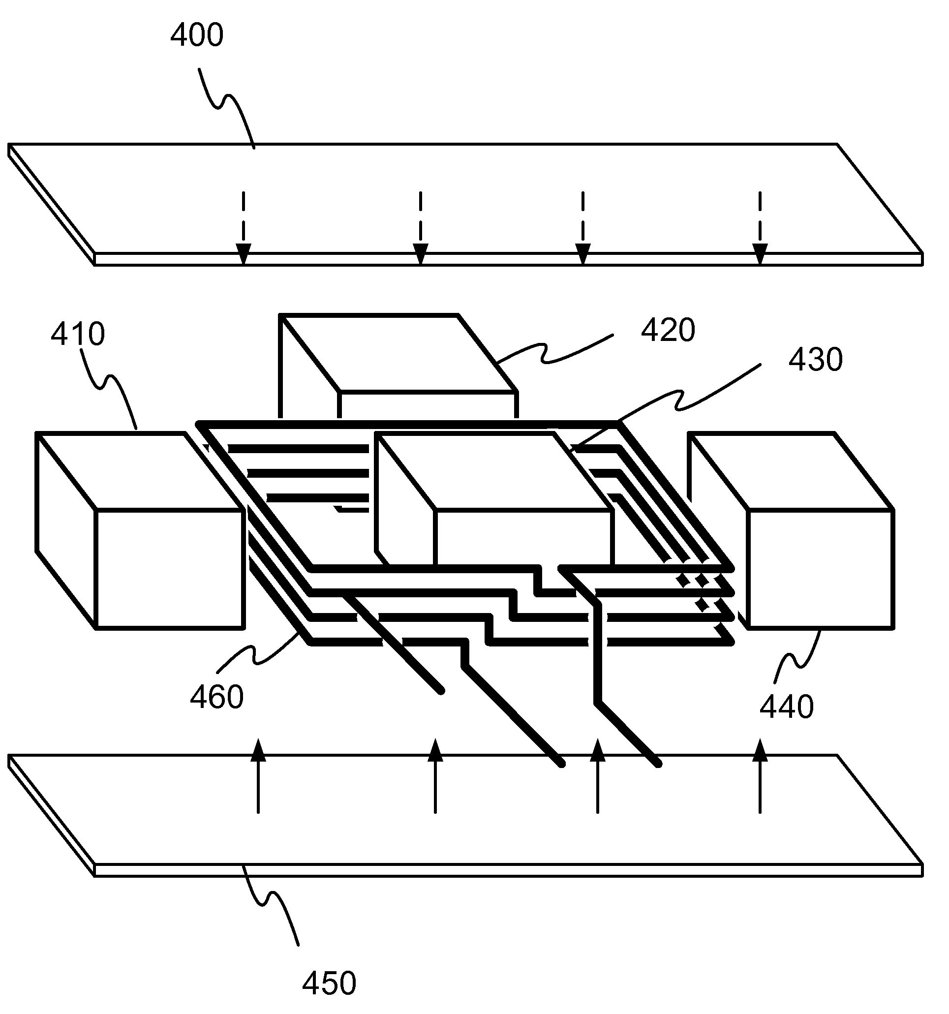
[0013]What we disclose is an enhancement to the inductance / area of on-chip inductance structures like T-coils and inductors. An embodiment of this invention enhances a T-coil as illustrated in this disclosure as well as generic BEOL inductors.

[0014]One embodiment uses silicon through via technology to create a via through the metal layers in a chip that is approximately 10-20 um in diameter. T-coil solutions show a center gap between the “coils” of metal of around 10-20 um.

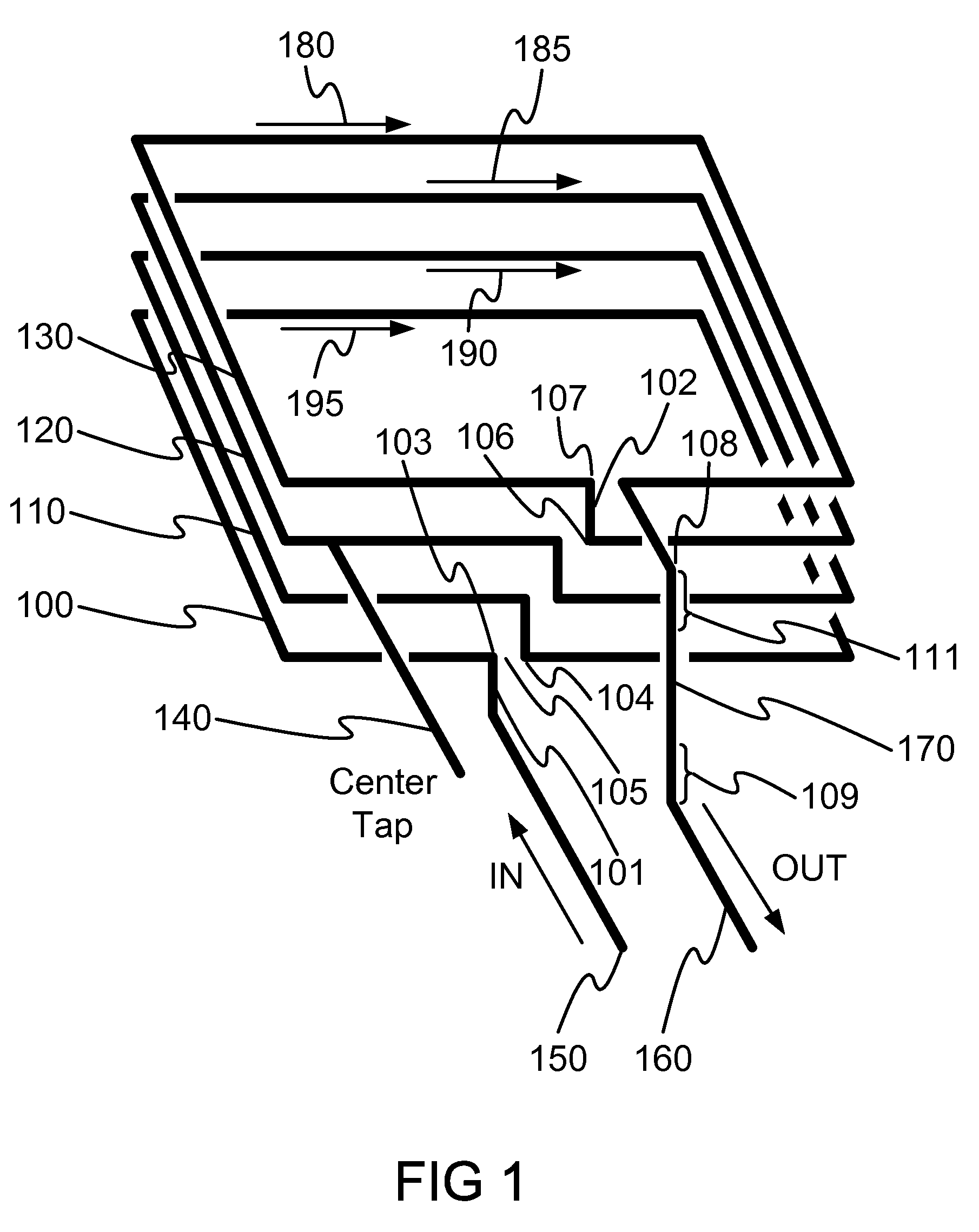
[0015]A layout example of a T-coil is shown in FIG. 1; the coil structure is constructed by Metal 1 (100), Metal 2 (110), Metal 3 (120) and Metal 4 (130). The stacked multi-ring structure depicted in FIG. 1, has an input electrode (150) and an output electrode (160). The output path in the Figure is depicted by the item (170) which connects to the output electrode and the Center Tap is shown as item (140). The current flow through the coil is shown by arrows (180, 185, 190 and 195).

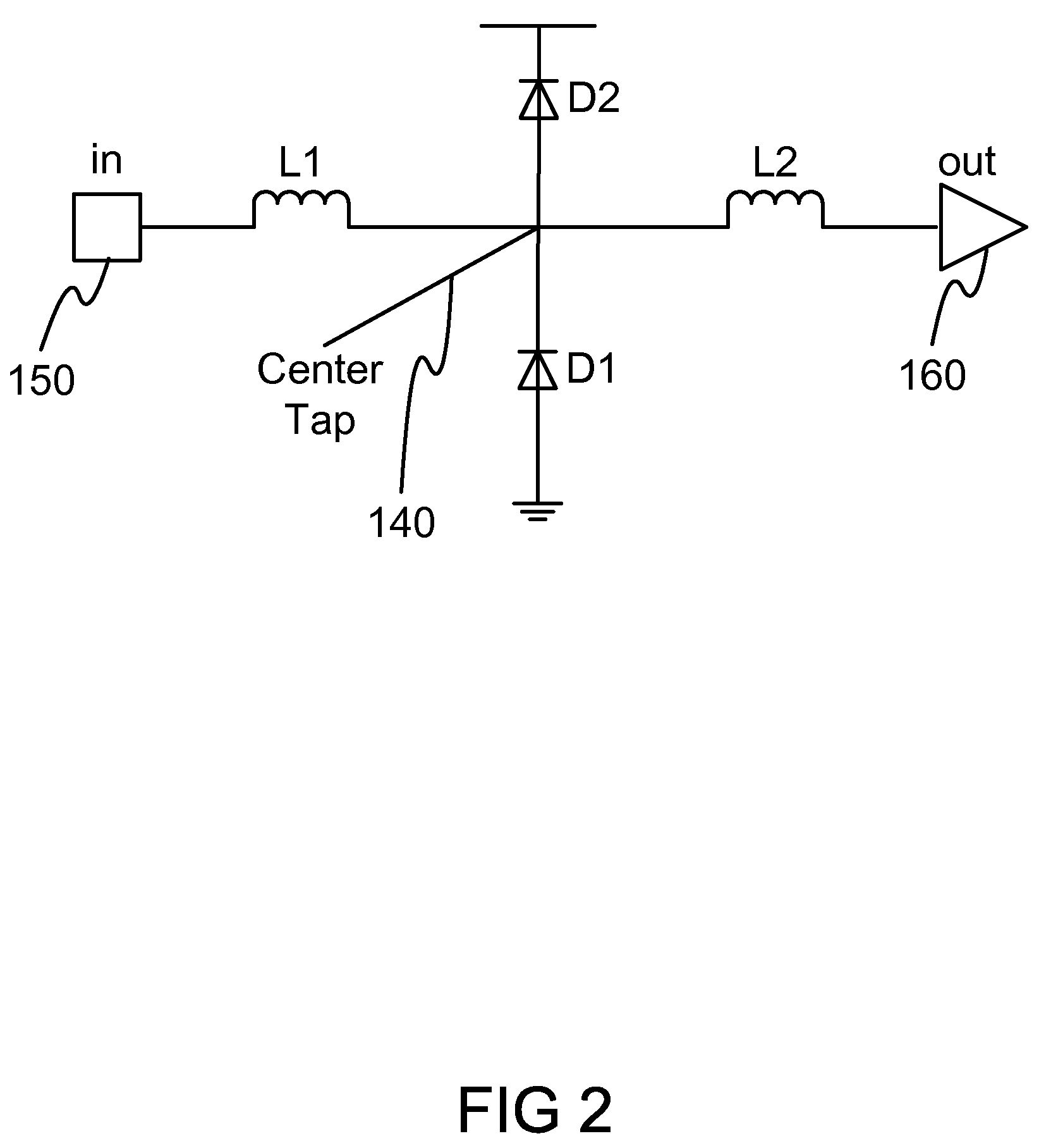
[0016]FIG. 2 shows a schematic d...


PUM

PropertyMeasurementUnit
diameteraaaaaaaaaa
inductanceaaaaaaaaaa
magneticaaaaaaaaaa

Abstract

A method is provided that utilizes silicon through via technology, to build a Toroid into the chip with the addition of a layer of magnetic material such as Nickel above and below the T-coil stacked multi-ring structure. This allows the connection between the inner via and an array of outer vias. This material is added on a BEOL metal layer or as an external coating on the finished silicon. Depending on the configuration and material used for the via, the inductance will increase approximately two orders of magnitude (e.g., by utilizing a nickel via core). Moreover, a ferrite material with proper thermal conduction properties is used in one embodiment.

Description

BACKGROUND OF THE INVENTION[0001]Use of on-chip inductance structures (e.g., T-coils and inductors) in VLSI design is becoming more prevalent as design frequencies increase. These structures are metal-only devices within a chip where “coils” of metal are created on wiring layers in an attempt to create inductance. This inductance is useful in high speed applications that are performance-limited due to capacitive loading. Due to its nature, these structures have a low inductance per unit area; a recent design demonstrated ˜1.5 nH per 2185 um2 of area. One can / may increase the inductance per unit area of silicon Back End Of Line (BEOL) inductance structures such as T-coils and inductors.[0002]The spiral of prior art does not allow for the use of external ferrites, and in the one instance does not have each coil of the spiral an equal distance from the core. Thus the flux linking thru the core is not optimized. Further, the prior art fundamentally provides for flux linkage thru horizon...

Claims


Application Information

Patent Timeline
Patent Type & Authority Patents(United States)
IPC IPC(8): H01F7/127B05D1/00
CPCH01F17/0013H01F17/06H01F41/046H01L28/10H01L23/5227H01F2021/125Y10T29/49073Y10T29/49075Y10T29/4902Y10T29/4906H01L2924/0002H01L2924/00
Inventor MAKI, ANDREW BENSONBARTLEY, GERALD KEITHGERMANN, PHILIP RAYMONDMAXSON, MARK OWENBECKER, DARRYL JOHNDAHLEN, PAUL ERICSHEETS, II, JOHN EDWARD
Owner INT BUSINESS MASCH CORP
Features
  • R&D
  • Intellectual Property
  • Life Sciences
  • Materials
  • Tech Scout
  • Unparalleled Data Quality
  • Higher Quality Content
  • 60% Fewer Hallucinations
Learn More