
Eureka
For R&D, Eureka makes reading and utilizing patents & technical documents easy.
Eureka AIR
Designed for self-driven R&D workflows. Generate viable solutions, solve complex R&D challenges, empower your innovation with AI.

Eureka Materials
Designed for material experts only. Revolutionize your material R&D, from search, analyze, to developing new materials.

TechResearch
Generate reliable direction feasibility study reports for your R&D in just a few steps.

TechSeek
Discover and master advanced knowledge NOW. Basics, ideas, possibilities, all at once.

TechMind
As an expert in R&D Theories, TechMind can generates customized viable solutions instantly.

TechRisk
Analyze your overall solution with one click, know your potential R&D risks in advance.

TechMonitor
Get weekly tech updates, stay abreast of the latest tech innovations and key insights.
Semiconductor device
a technology of semiconductors and devices, applied in pulse manipulation, pulse techniques, instruments, etc., can solve the problems of complex configuration and slow signal writing speed, and achieve the effect of slowing down signal writing speed
- Summary
- Abstract
- Description
- Claims
- Application Information
AI Technical Summary
Benefits of technology
Problems solved by technology
Method used
Image

Examples
embodiment mode 1
[0087]According to the invention, a pixel is configured with an element enable to control a luminance based on a current value flowing through a light emitting element. Typically, an EL element can be used. There are various known configurations of the EL element and any element configuration may be used in the invention so long as luminance thereof can be controlled based on a current value. That is, an EL element is formed by freely combining a light emitting layer, a charge transporting layer and a charge injecting layer. As a material for the EL element, a low-molecular weight organic material, a medium-molecular weight organic material (an organic light emitting material which has no sublimation property and in which the number of molecules is 20 or less or a length of chained molecules is 10 m or less), or a polymer organic material can be employed. Alternatively, each of the organic materials may be mixed or dispersed with an inorganic material.
[0088]According to the inventio...
embodiment mode 2
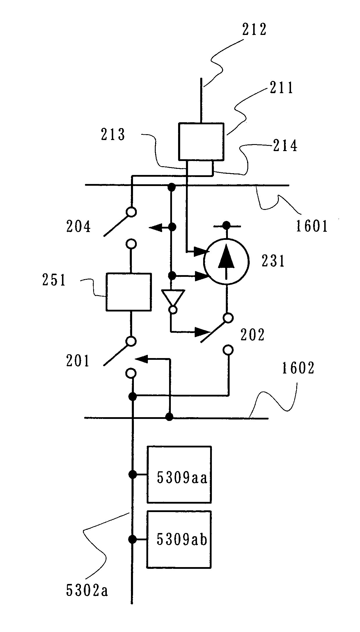
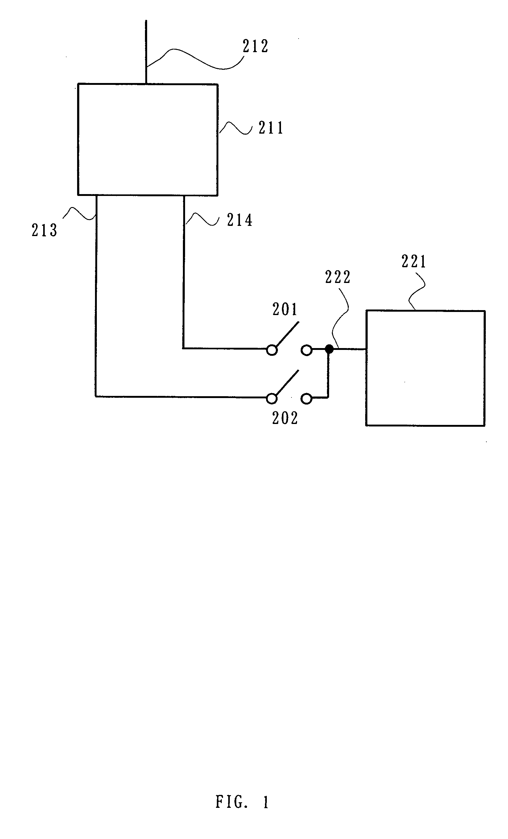
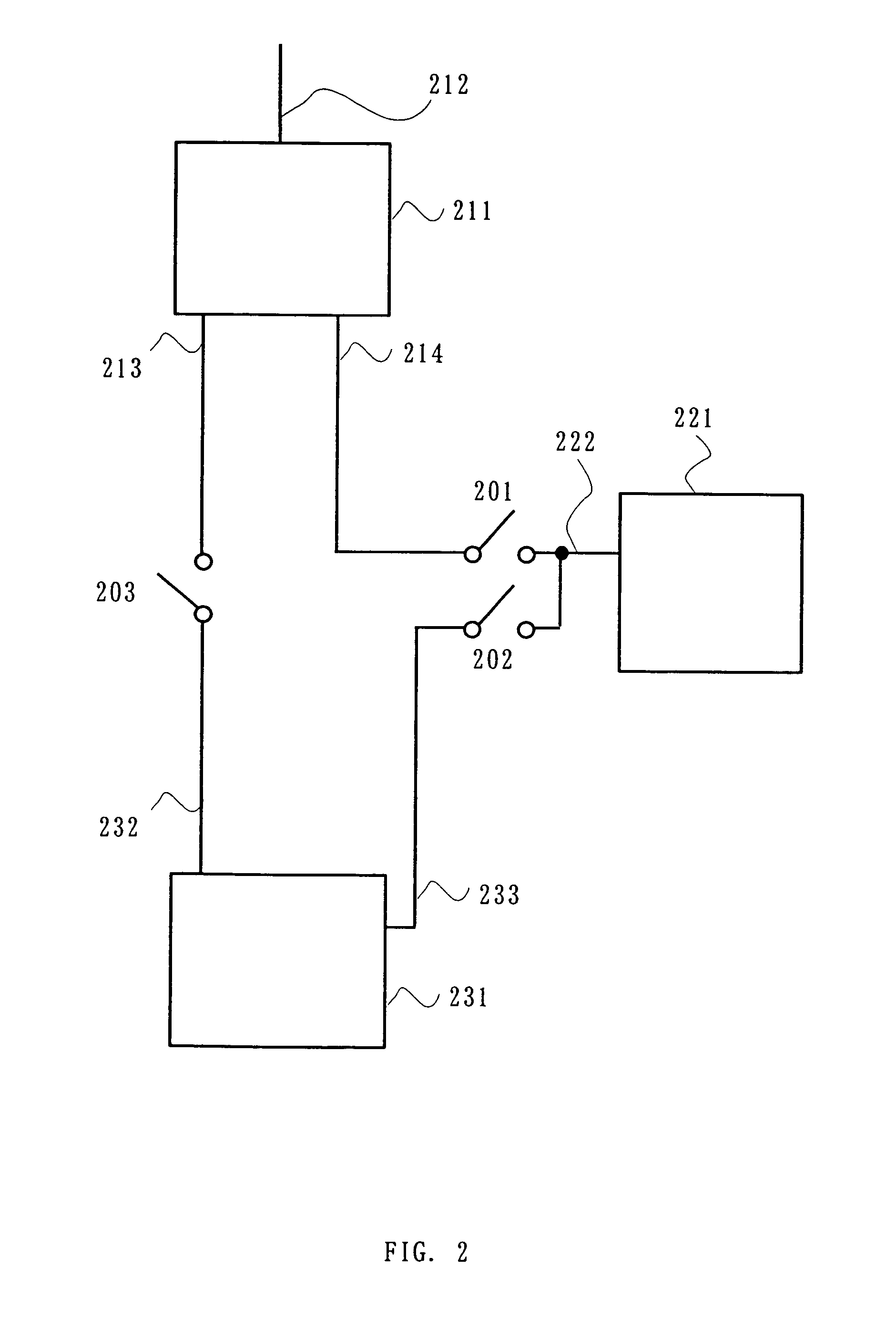
[0154]In Embodiment Mode 1, the case of connecting circuits to one signal line, that is, the case for one column is described. In the case of disposing a plurality of columns, pixels are disposed in a two-dimensional manner and a plurality of circuits 211 for supplying voltage and current are provided as well.
[0155]In the case where a plurality of the circuits 211 for supplying voltage and current are provided, it is necessary to supply a signal to the original signal input terminal 212 of each circuit 211 for supplying voltage and current. Described below is a driver circuit for controlling the signal supply to the original signal input terminal 212 of each circuit 211 for supplying voltage and current.
[0156]FIG. 31 shows the most standard driver circuit. Described here is the case where the circuits for supplying voltage and current for three columns are provide for simplicity. The circuits 211a to 211c for supplying voltage and current are connected to an original signal supply l...
embodiment mode 3
[0178]Electronic apparatuses each using the invention include a video camera, a digital camera, a goggle type display (a head mount display), a navigation system, a sound reproducing device (a car audio equipment and an audio set), a lap-top computer, a game machine, a portable information terminal (a mobile computer, a mobile phone, a portable game machine, an electronic book, and the like), an image reproducing device including a recording medium (more specifically, a device which can reproduce a recording medium such as a digital versatile disc (DVD) and display the reproduced image), or the like. Specific examples of those electric apparatuses are shown in FIGS. 50A to 50H.
[0179]FIG. 50A shows a light emitting device, which includes a housing 13001, a support base 13002, a display portion 13003, speaker portions 13004, a video input terminal 13005, and the like. The invention can be applied to an electronic circuit configuring the display portion 13003. The light emitting device...
PUM
 Abstract
Description
Claims
Application Information
 - R&D Engineer
- R&D Manager
- IP Professional
- Industry Leading Data Capabilities
- Powerful AI technology
- Patent DNA Extraction
Browse by: Latest US Patents, China's latest patents, Technical Efficacy Thesaurus, Application Domain, Technology Topic, Popular Technical Reports.
© 2024 PatSnap. All rights reserved.Legal|Privacy policy|Modern Slavery Act Transparency Statement|Sitemap|About US| Contact US: help@patsnap.com