Eureka AIR delivers breakthrough ideas for toughest innovation challenges, trusted by R&D personnel around the world.

Semiconductor device

Inactive Publication Date: 2005-02-17
SEMICON ENERGY LAB CO LTD
View PDF19 Cites 2 Cited by
  • Summary
  • Abstract
  • Description
  • Claims
  • Application Information

AI Technical Summary

Benefits of technology

[0028] However, as the parasitic capacitance of a wiring used for supplying a signal current to a driving TFT and a light emitting element is quite large, a time constant for charging the parasitic capacitance of the wiring becomes large in the case of small signal current, which slows down the signal writing speed. That is, even when a signal current is supplied to a transistor, it takes long to generate a voltage required for flowing the signal current at a gate terminal thereof, therefore the signal writing speed is slowed down.
[0030] In view of the foregoing problems, it is an object of the invention to provide a semiconductor device in which the influence of characteristic variations of transistors is reduced and a predetermined current can be supplied, so that the signal writing speed can be sufficiently improved even when a signal current is small.

Problems solved by technology

However, as the parasitic capacitance of a wiring used for supplying a signal current to a driving TFT and a light emitting element is quite large, a time constant for charging the parasitic capacitance of the wiring becomes large in the case of small signal current, which slows down the signal writing speed.
In addition, the configuration is complex.

Method used


Image

  • Semiconductor device
  • Semiconductor device
  • Semiconductor device

Examples


embodiment

[0160] [Embodiment Mode 2]

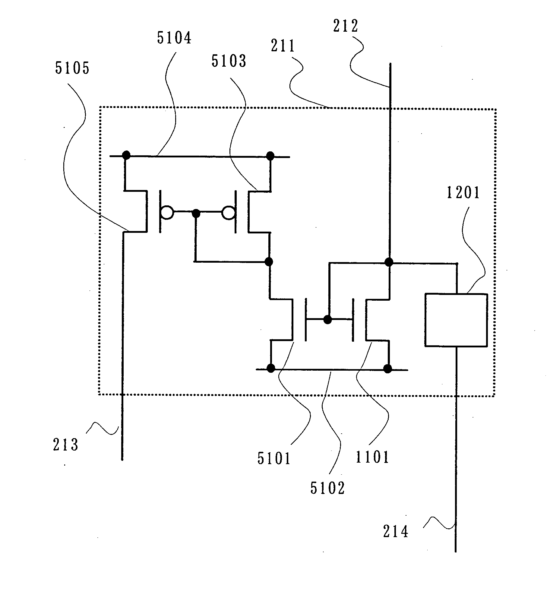
[0161] In Embodiment Mode 1, the case of connecting circuits to one signal line, that is, the case for one column is described. In the case of disposing a plurality of columns, pixels are disposed in a two-dimensional manner and a plurality of circuits 211 for supplying voltage and current are provided as well.

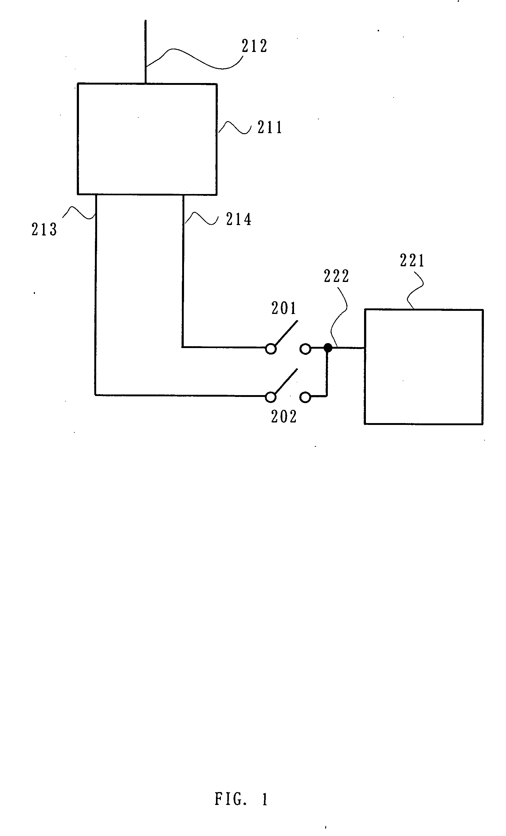
[0162] In the case where a plurality of the circuits 211 for supplying voltage and current are provided, it is necessary to supply a signal to the original signal input terminal 212 of each circuit 211 for supplying voltage and current. Described below is a driver circuit for controlling the signal supply to the original signal input terminal 212 of each circuit 211 for supplying voltage and current.

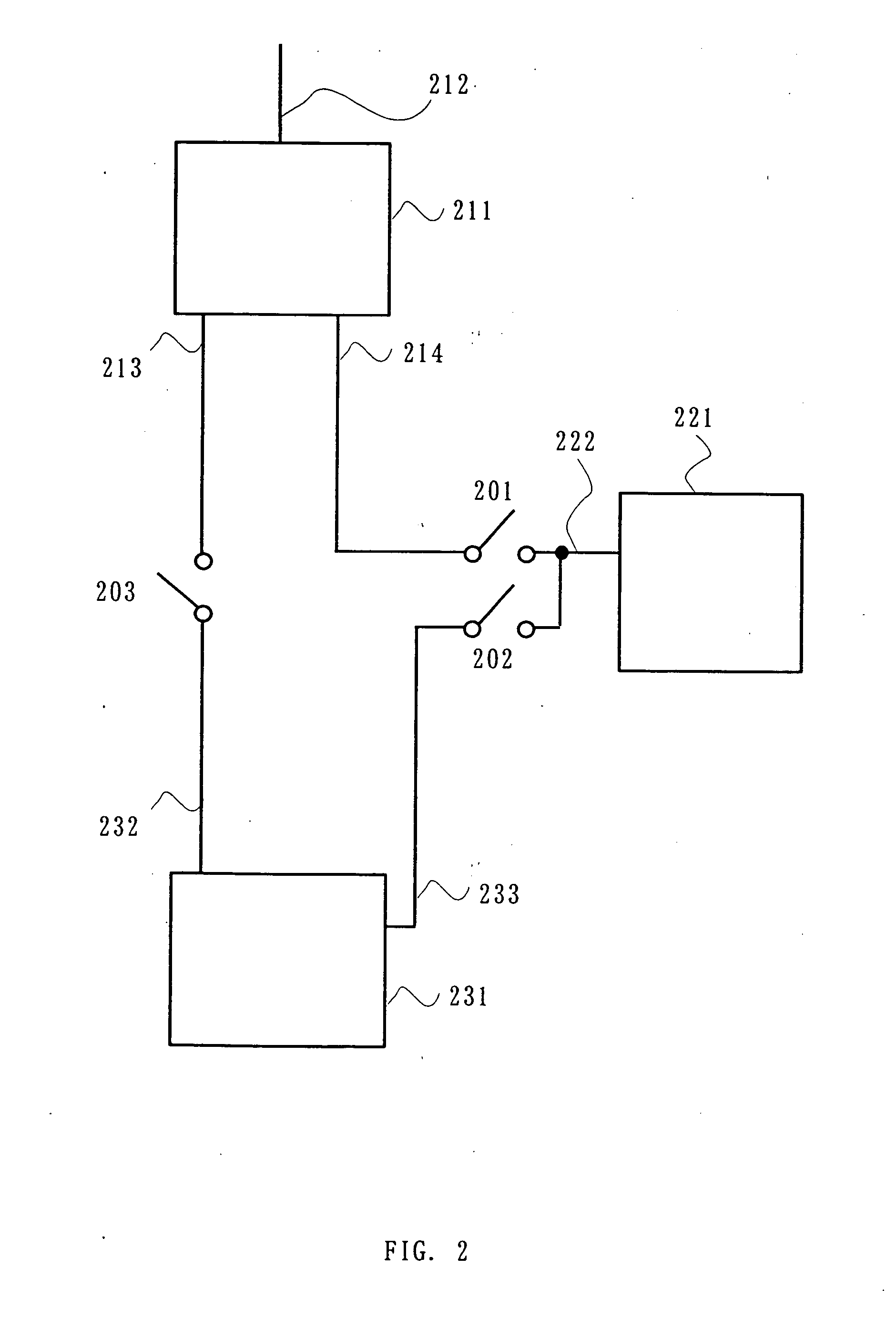
[0163]FIG. 31 shows the most standard driver circuit. Described here is the case where the circuits for supplying voltage and current for three columns are provide for simplicity. The circuits 211a to 211c for supplying voltage and current are connected ...


PUM


Abstract

A semiconductor device with a transistor for supplying a current to a pixel comprising an EL element, that can supply an accurate current without the influence of variations even when a small signal current, is provided. A precharge voltage is supplied in advance for the current supply to a pixel and subsequently, the signal writing is completed quickly. The precharge voltage is outputted from a circuit for supplying voltage and current that supplies a current to a current source circuit for supplying a current to the pixel. As the precharge voltage, a gate voltage of a transistor for supplying a current to the current source circuit is supplied to the pixel. Optimum precharge voltage can be supplied in the case where W / L of a transistor in the pixel and W / L of a transistor for supplying current in the circuit for supplying voltage and current are approximately equivalent to each other.

Description

BACKGROUND OF THE INVENTION [0001] 1. Field of the Invention [0002] The present invention relates to a semiconductor device which is provided with a function of controlling a current supplied to a load by a transistor, and more particularly to a semiconductor device comprising a pixel comprising a current drive type light emitting element whose luminance varies with current, and a circuit for supplying a signal to the pixel. [0003] 2. Description of the Related Art [0004] As a display device using a self-light emitting element typified by an organic light emitting diode (OLED, which is also referred to as an organic EL element, an electroluminescence (EL) element, and the like), there are two types: a passive matrix and an active matrix according to a driving method thereof. The passive matrix display device has a simple configuration while it has a difficulty in realizing a display with a large size and high luminance. In recent years, an active matrix display device in which a cur...

Claims


Application Information

Patent Timeline
IPC IPC(8): G09G3/32G11C27/02H03K5/00H03K5/24H05B44/00
CPCG09G3/3241G09G3/325G09G3/3283H03K5/2472G09G2300/0861G09G2310/0251G11C27/028G09G2300/0842
Inventor KIMURA, HAJIME
Owner SEMICON ENERGY LAB CO LTD
Why Eureka
Eureka Blog
Learn More