Check patentability & draft patents in minutes with Patsnap Eureka AI!

Apparatus and method of avoiding bank conflict in single-port multi-bank memory system

a multi-bank memory and apparatus technology, applied in the field of data access to a memory, can solve the problems of deteriorating processor performance, bank conflict, and inability to access multiple load/store units, so as to avoid bank conflict, avoid bank conflict, avoid bank conflict

Active Publication Date: 2012-07-03
SAMSUNG ELECTRONICS CO LTD
View PDF12 Cites 2 Cited by
  • Summary
  • Abstract
  • Description
  • Claims
  • Application Information

AI Technical Summary

Benefits of technology

The present invention provides an apparatus, method, and computer-readable medium for avoiding bank conflict when a bank conflict is predicted. The apparatus includes a scheduling unit that replaces a first instruction that instructs a load / store unit to access the same bank with a second instruction that changes the execute timing of the first instruction. The second instruction allows another load / store unit to access the same bank without interfering with the first instruction. The method and computer-readable medium allow for efficient and effective avoidance of bank conflict, reducing the likelihood of system failure and improving overall performance.

Problems solved by technology

That is, one bank cannot be accessed by multiple load / store units.
However, there are some cases where multiple load / store units need to access the same bank.
In these cases, bank conflict occurs.
Frequent occurrence of bank conflict is one of the main causes of deterioration in performance of the processor.

Method used


Image

  • Apparatus and method of avoiding bank conflict in single-port multi-bank memory system
  • Apparatus and method of avoiding bank conflict in single-port multi-bank memory system
  • Apparatus and method of avoiding bank conflict in single-port multi-bank memory system

Examples


Embodiment Construction

[0024]The attached drawings for illustrating exemplary embodiments of the present invention are referred to in order to gain a sufficient understanding of the present invention, the merits thereof, and the objectives accomplished by the implementation of the present invention.

[0025]Hereinafter, an apparatus and method of avoiding bank conflict will be described with reference to the accompanying drawings.

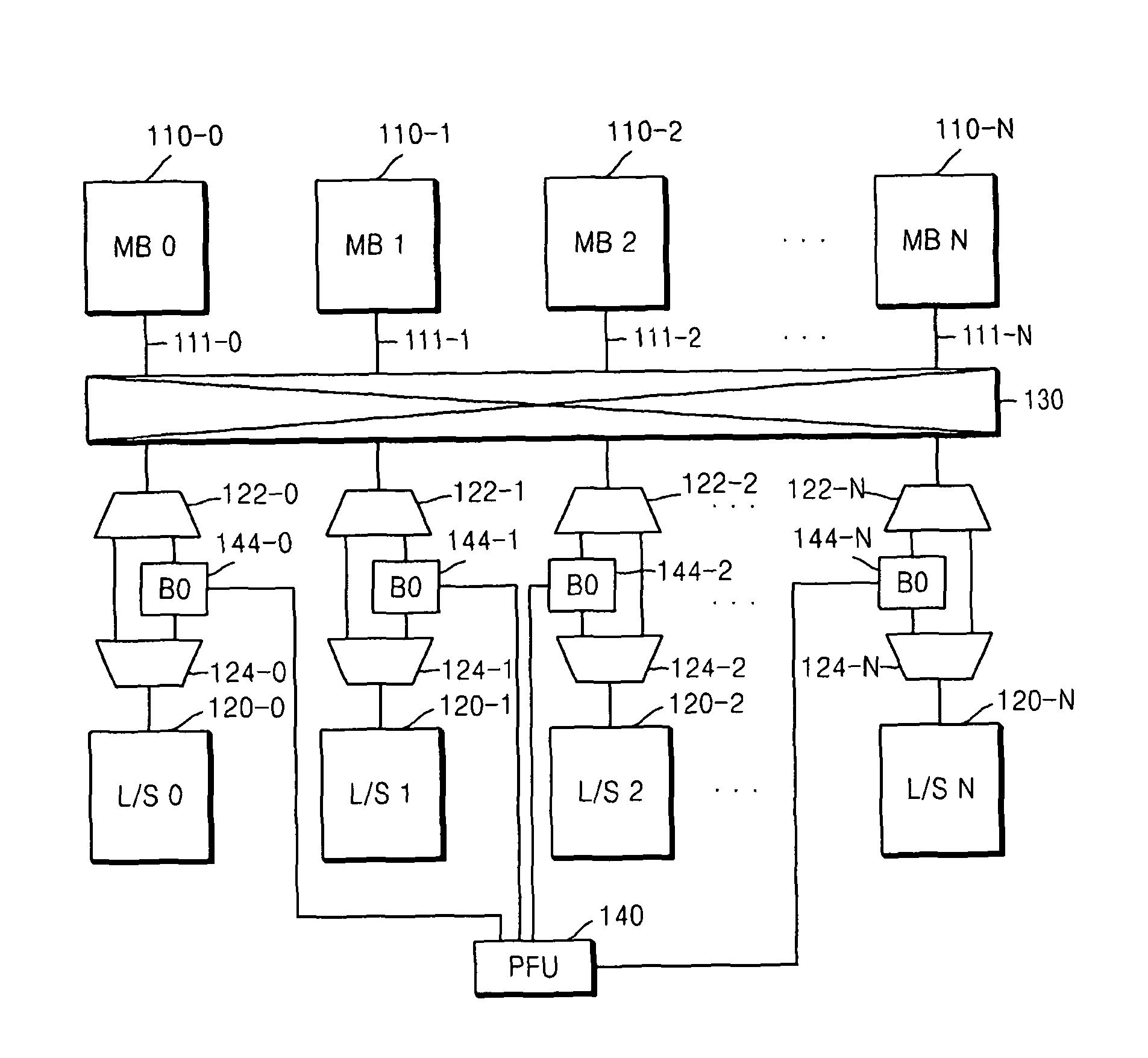
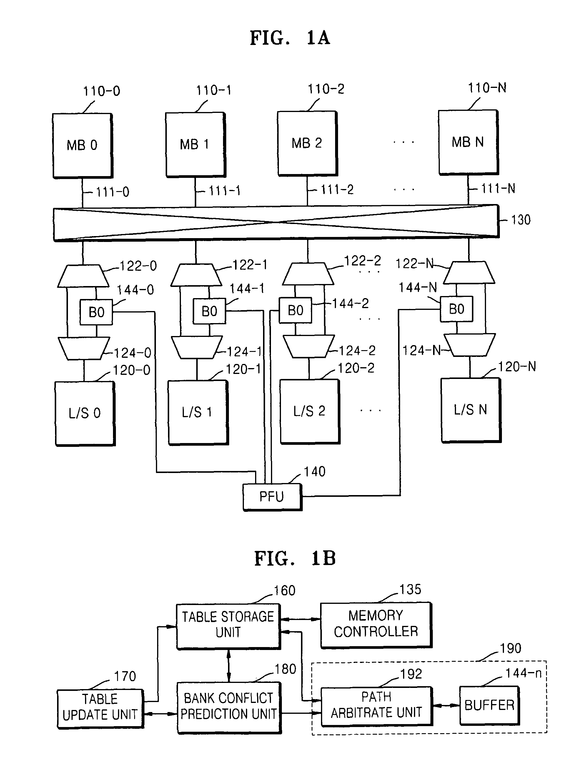
[0026]FIG. 1A is a circuit diagram for explaining an apparatus for avoiding bank conflict according to the present invention. FIG. 1B is a block diagram for explaining the apparatus for avoiding bank conflict according to the present invention. Referring to FIGS. 1A and 1B, the apparatus for avoiding bank conflict according to the present invention includes one or more banks MB0, MB1, MB2, . . . , and MBM (110-0, 110-1, 110-2, . . . , and 110-M) (M is a non-negative integer), a processor including a plurality of load / store units L / S0, L / S1, L / S2, . . . , and L / SN (120-0, 120-1, 120-...


PUM


Abstract

Provided are a method and apparatus for avoiding bank conflict. A first instruction that is one of access instructions that are predicted to cause the bank conflict is replaced with a second instruction by changing an execute timing of the first instruction to a timing prior to the execute timing of the first instruction so as for the access instructions not to cause the bank conflict. Next, a load / store unit that is scheduled to access the bank according to the first instruction accesses the bank and reads out a data from the bank at an execute timing of the second instruction, and after that, the load / store unit is allowed to be inputted the read data at the execute timing of the first instruction. Accordingly, although the access instructions that are predicted to cause the bank conflict are allocated to the load / store units, the bank conflict can be prevented, so that it is possible to avoid deterioration in performance due the occurrence of the bank conflict.

Description

CROSS-REFERENCE TO RELATED PATENT APPLICATION[0001]This application claims the priority of Korean Patent Application No. 2007-0098952, filed on Oct. 1, 2007, in the Korean Intellectual Property Office, the disclosure of which is incorporated herein in its entirety by reference.BACKGROUND OF THE INVENTION[0002]1. Field of the Invention[0003]The present invention relates to data access to a memory, and more particularly, to an apparatus and method of controlling access to single-port multi-bank memory system.[0004]2. Description of the Related Art[0005]Recently, with increasing demands for processors capable of simultaneously processing a large amount of data, some of the processors have been designed to simultaneously access multiple banks. Such a process includes multiple load / store units, each of which can access one bank. One bank is accessed by only one load / store unit. That is, one bank cannot be accessed by multiple load / store units.[0006]However, there are some cases where mul...

Claims


Application Information

Patent Timeline
Patent Type & Authority Patents(United States)
IPC IPC(8): G06F12/00
CPCG06F9/30043G06F9/3836G06F9/3824G06F12/00G06F13/16G11C7/00
Inventor MIN, KYOUNG-JUNEPARK, CHAN-MINKIM, SUK-JINLEE, WON-JONGKWON, KWON-TAEKKIM, HEE-SEOK
Owner SAMSUNG ELECTRONICS CO LTD
Features
  • R&D
  • Intellectual Property
  • Life Sciences
  • Materials
  • Tech Scout
  • Unparalleled Data Quality
  • Higher Quality Content
  • 60% Fewer Hallucinations
Learn More