Method for producing a stack of semi-conductor thin films

a technology of semi-conductor thin films and stacks, which is applied in the manufacture of semiconductor/solid-state devices, basic electric elements, electric devices, etc., can solve the problems of reducing the dimension of the oxide layer, forming defects at the bonding interface, and affecting the final semi-conductor structure, so as to reduce the exposure time of the device

Active Publication Date: 2013-08-20
SOITEC SA
View PDF14 Cites 3 Cited by
  • Summary
  • Abstract
  • Description
  • Claims
  • Application Information

AI Technical Summary

Benefits of technology

[0020]The insulator-insulator bonding thus carried out makes it possible to reduce production kinetic of hydrogen and thus limit the formation of blisters. Indeed, the molecules of H2O introduced at the bonding interface during the assembly are included between two insulator layers; before reacting with the material of one of the substrates to form hydrogen radicals, the molecules of water have to pass through these insulator layers. Thus the oxide layers, having a property of barrier to the diffusion of H2O or limiting this diffusion, slow down the formation of hydrogen and thus blisters, which improves the reliability of the semi-conductor structures thereby formed.
[0030]A heat treatment, known as annealing, with a temperature between 700° C. and 1300° C., preferentially between 900° C. and 1200° C. and with a temperature increase ramp greater than 10° C. / s or advantageously greater than 20° C. / s may be applied after the thinning so as to consolidate the bonding interface and minimise the exposure time of the device to temperatures between 400° C. and 700° C. and advantageously between 400° C. and 900° C., which correspond to the temperature range in which the blisters formation kinetic is high and is the least favourable to the quality of the final semi-conductor structure.
[0031]Annealing at a temperature above 700° C. or preferentially above 900° C. enables an evacuation of the captive hydrogen, present at the bonding interface or at the interfaces between the substrates and the oxide layers, by diffusion in the semi-conductor material.
[0032]In the temperature interval 400° C.-900° C., for silicon, there is formation of blisters due to the release of gaseous hydrogen. The resulting pressure deforms the materials of the two bonded substrates and forms blisters and may cause the rupture of the final structure during subsequent treatments or during the fracture heat treatment of the substrate or consolidation heat treatment. A high temperature ramp, as mentioned above (at least 10° C. / s), makes it possible to minimise the passage in this critical temperature interval and thus makes it possible to attain the temperature of diffusion of hydrogen in the semi-conductor material (close to 900° C.) before the pressure in the blisters weakens the device in an irremediable manner.
[0035]minimise the thermal treatment times included in the critical temperature interval.
[0036]Tests can enable to identify the critical temperature interval more precisely if a method according to the invention is applied.

Problems solved by technology

In the field of the manufacturing of SOI-like structures, comprising a thin film of buried oxide (less than 1 μm) contained between a thin film of semi-conductor material and a final substrate, one of the major problems that appear during the reduction of the dimensions of the oxide layer is the formation of defects at the bonding interface.
The presence of these defects may be fatal for the final semi-conductor structure.
This shows that the production of UTBOX structures according to the known method from the prior art is difficult for thicknesses of oxide in the order of 30 nm or less.
But this solution prevents the consolidation of the bonding interface, which has to take place at a temperature above 400° C., in general around 700° C. to 1300° C. In addition, this method limits the types of processes permitted during the industrial use of the device thereby obtained, and this thus limits the applications of such a UTBOX device.

Method used


Image

  • Method for producing a stack of semi-conductor thin films
  • Method for producing a stack of semi-conductor thin films
  • Method for producing a stack of semi-conductor thin films

Examples


Embodiment Construction

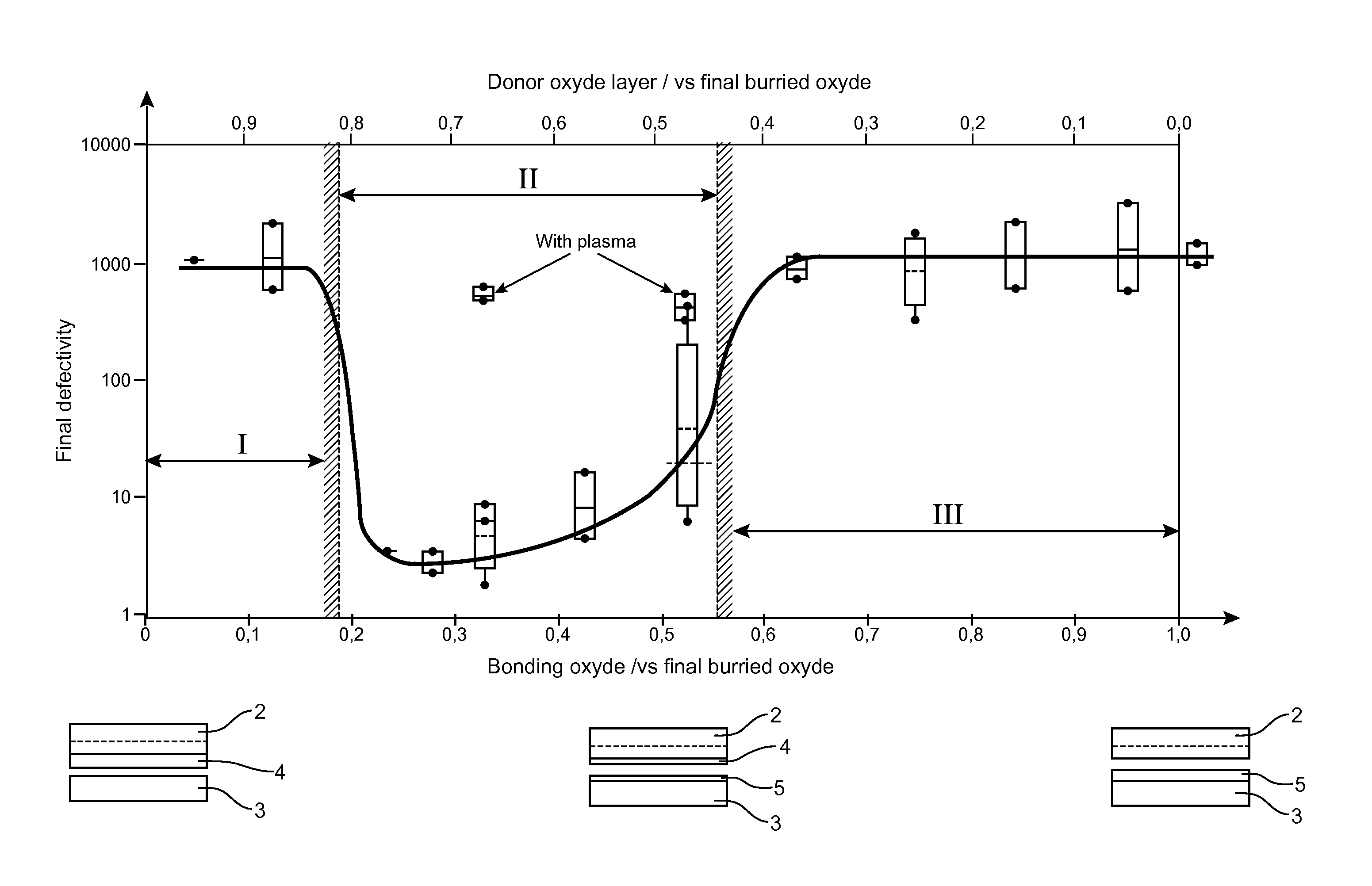
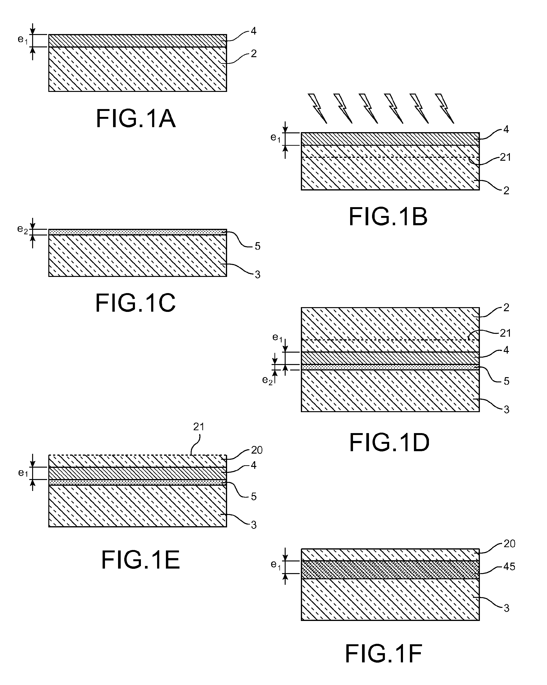
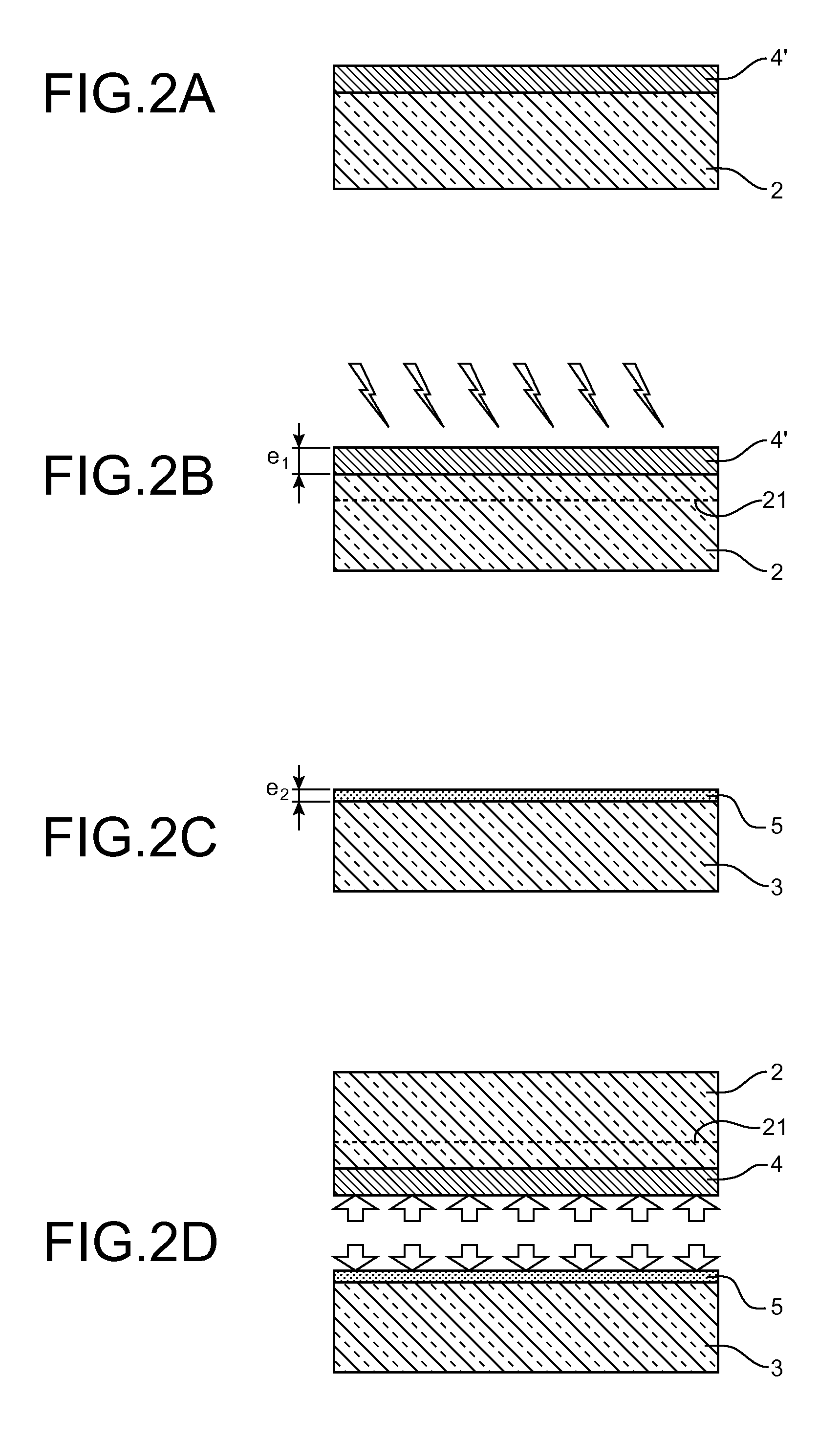
[0041]The invention relates to a method for producing systems of stacked SOI type semi-conductor layers and, more specifically, UTBOX type, in other words with ultra thin thickness of buried insulator layer.

[0042]The method is illustrated according to two embodiments in FIGS. 1A to 1F and 2A to 2G, any reference corresponding to a same element in the different figures.

[0043]The first embodiment (FIGS. 1A to 1F) relates to a method for producing SOI structures with thin buried insulator layer, thinner than 50 nm; advantageously this insulator layer is less than 20 nm, and preferentially less than 15 nm, it may also be less than 10 or 7 nm.

[0044]The insulator is preferentially an electrical insulator, it may be a nitride layer or may advantageously be an oxide layer, for example a silicon oxide. In the remainder of the description, the example of oxide layers is taken but this is not limitative. As explained previously, in a method according to the invention, during the bonding, the i...


PUM


Abstract

A method for producing a stacked structure having an ultra thin buried oxide (UTBOX) layer therein by forming an electrical insulator layer on a donor substrate, introducing elements into the donor substrate through the insulator layer, forming an electrical insulator layer, on a second substrate, and bonding the two substrates together to form the stack, with the two insulator layers limiting the diffusion of water and forming the UTBOX layer between the two substrates at a thickness of less than 50 nm, wherein the donor oxide layer has, during bonding, a thickness at least equal to that of the bonding oxide layer.

Description

[0001]This application is a 371 filing of International Patent Application PCT / EP2009 / 064307 filed Oct. 29, 2009.TECHNICAL FIELD AND PRIOR ART[0002]In the field of the manufacturing of SOI-like structures, comprising a thin film of buried oxide (less than 1 μm) contained between a thin film of semi-conductor material and a final substrate, one of the major problems that appear during the reduction of the dimensions of the oxide layer is the formation of defects at the bonding interface.[0003]The presence of these defects may be fatal for the final semi-conductor structure. Some of these defects, hydrogen blisters, appear during temperature annealings (S. Mack et al. Journal of Electrochemical Society. Vol. 144, p. 1106, 1997).[0004]In contact with the semi-conductor material of any of the two substrates, the molecules of water brought to the bonding interface during the molecular bonding are going to react with the materials of the substrates and produce hydrogen, or any other react...

Claims


Application Information

Patent Timeline
Patent Type & Authority Patents(United States)
IPC IPC(8): H01L21/48
CPCH01L21/76254
Inventor LANDRU, DIDIER
Owner SOITEC SA
Why Eureka
Try Eureka