

Method for producing a stack of semi-conductor thin films
a technology of semi-conductor thin films and stacks, which is applied in the manufacture of semiconductor/solid-state devices, basic electric elements, electric devices, etc., can solve the problems of reducing the dimensions of the oxide layer, forming defects at the bonding interface, and causing the death of the final semi-conductor structur
Active Publication Date: 2011-07-21
SOITEC SA
View PDF10 Cites 8 Cited by
- Summary
- Abstract
- Description
- Claims
- Application Information
AI Technical Summary
Benefits of technology
The invention proposes a method for improving the reliability of UTBOX structure semi-conductor devices by reducing the formation of blisters and improving the bonding of insulator layers. The method involves the use of insulator layers that form a barrier to the diffusion of water and limit the formation of hydrogen. The insulator layers are formed on the substrates before assembly, and a bonding oxide layer is formed on the substrates to further limit the formation of blisters. The method also includes steps of cleaning and etching the substrates. The invention aims to improve the production kinetics of hydrogen and thus reduce the formation of blisters in the final device.
Problems solved by technology
In the field of the manufacturing of SOI-like structures, comprising a thin film of buried oxide (less than 1 μm) contained between a thin film of semi-conductor material and a final substrate, one of the major problems that appear during the reduction of the dimensions of the oxide layer is the formation of defects at the bonding interface.
The presence of these defects may be fatal for the final semi-conductor structure.
This shows that the production of UTBOX structures according to the known method from the prior art is difficult for thicknesses of oxide in the order of 30 nm or less.
But this solution prevents the consolidation of the bonding interface, which has to take place at a temperature above 400° C., in general around 700° C. to 1300° C. In addition, this method limits the types of processes permitted during the industrial use of the device thereby obtained, and this thus limits the applications of such a UTBOX device.
Method used
View moreImage
Smart ImageViewing Examples

Examples
first embodiment
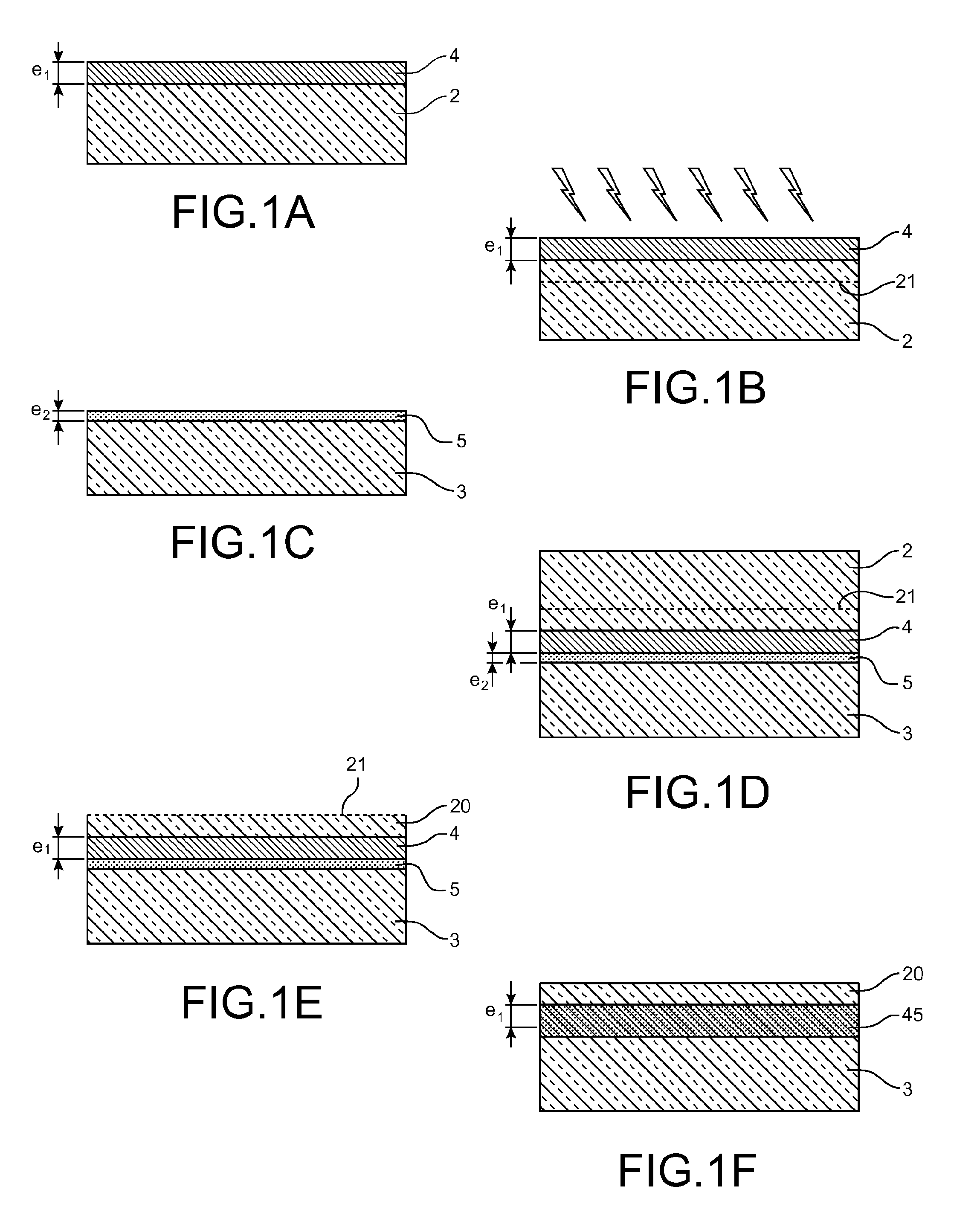
[0036]FIGS. 1A to 1F represent a method according to the invention.
second embodiment
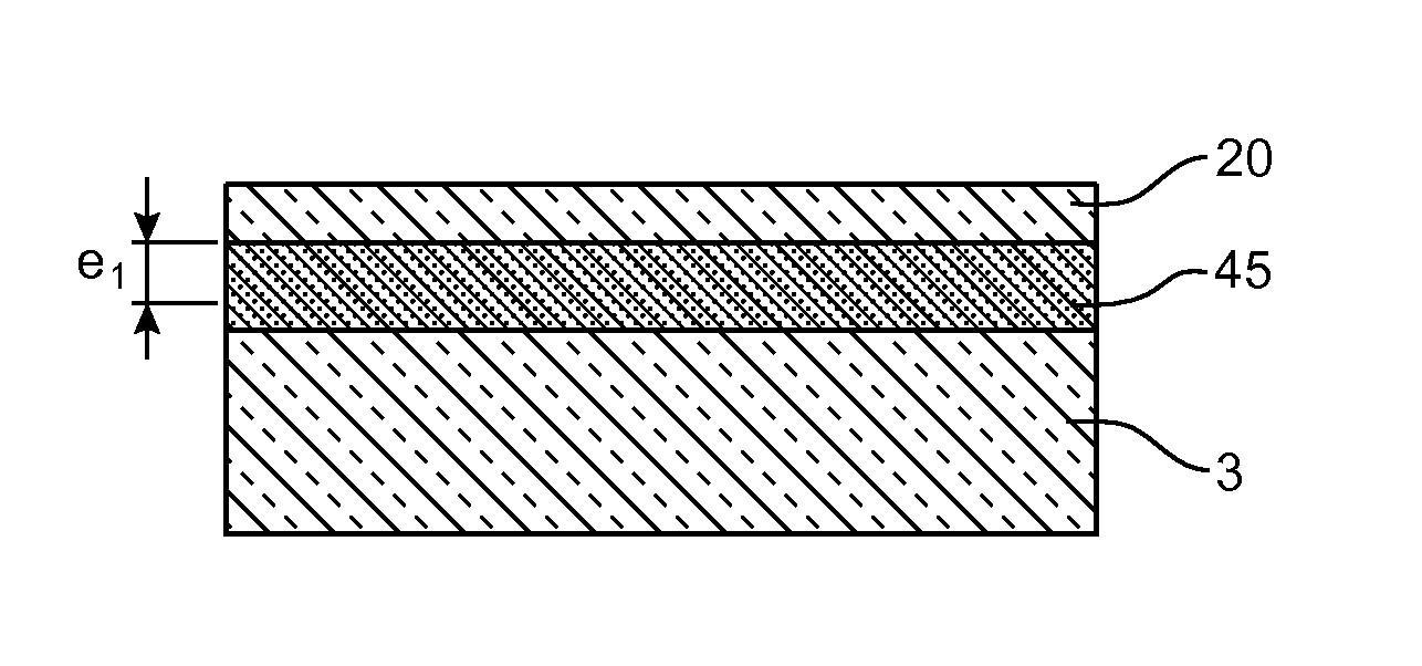
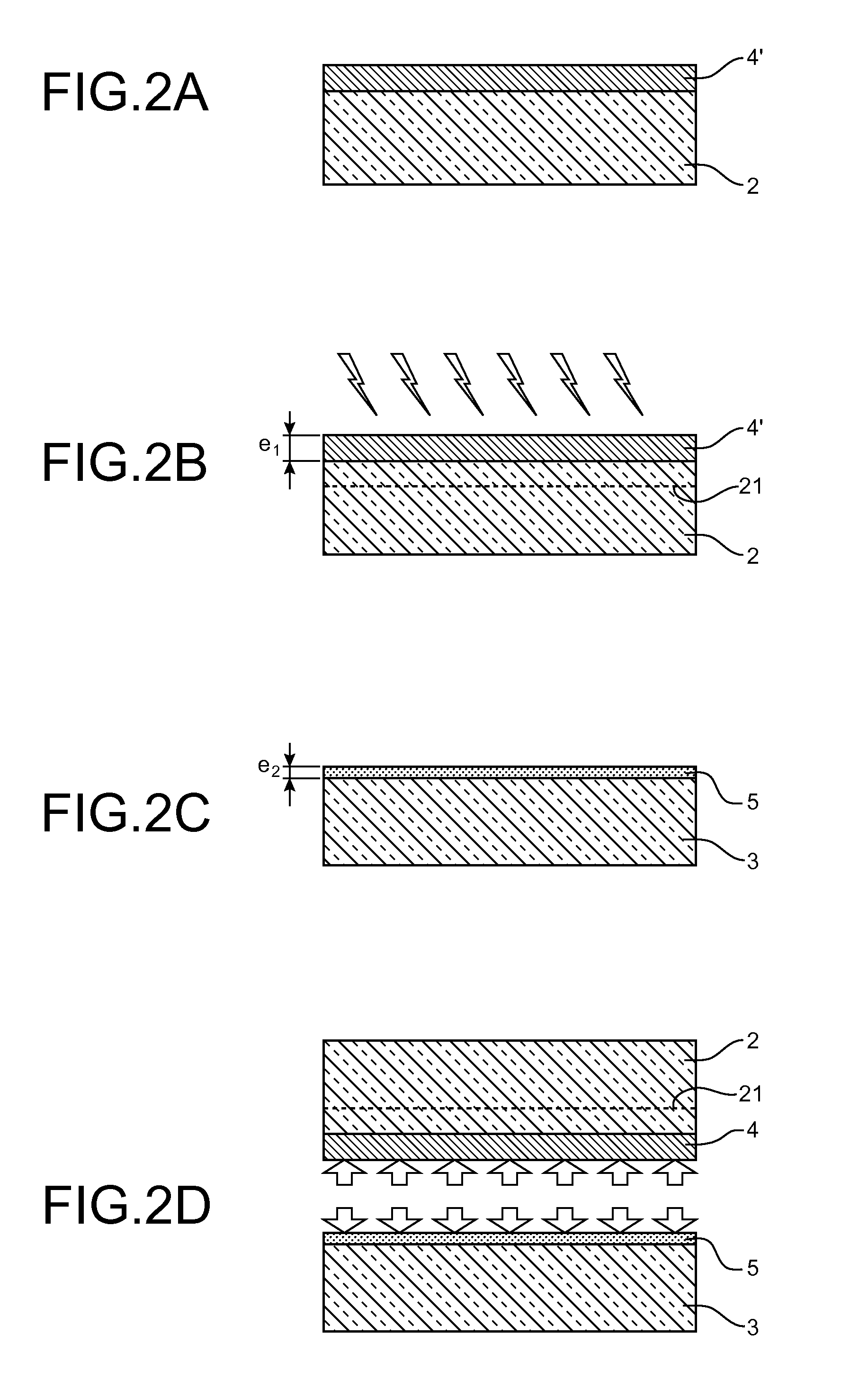
[0037]FIGS. 2A to 2G represent a method according to the invention, in which thicknesses of oxide higher than the requisite thickness for the final device are formed.
[0038]FIG. 3 illustrates results of defectiveness experiments obtained by the inventors as a function of the ratios of the thicknesses of the oxide layers compared to the final thickness of oxide in the case of SiO2 and silicon substrates.
[0039]FIG. 4 illustrates results of defectiveness experiments as a function of the thickness of the final oxide layer, obtained by the inventors and showing the efficiency of a method according to the invention to create UTBOX structures having a low oxide thickness.
Login to View More PUM
 Abstract
A method for producing a stacked structure having an ultra thin buried oxide (UTBOX) layer therein by forming an electrical insulator layer on a donor substrate, introducing elements into the donor substrate through the insulator layer, forming an electrical insulator layer, on a second substrate, and bonding the two substrates together to form the stack, with the two insulator layers limiting the diffusion of water and forming the UTBOX layer between the two substrates at a thickness of less than 50 nm, wherein the donor oxide layer has, during bonding, a thickness at least equal to that of the bonding oxide layer.
Description
TECHNICAL FIELD AND PRIOR ART[0001]In the field of the manufacturing of SOI-like structures, comprising a thin film of buried oxide (less than 1 μm) contained between a thin film of semi-conductor material and a final substrate, one of the major problems that appear during the reduction of the dimensions of the oxide layer is the formation of defects at the bonding interface.[0002]The presence of these defects may be fatal for the final semi-conductor structure. Some of these defects, hydrogen blisters, appear during temperature annealings (S. Mack et al. Journal of Electrochemical Society. Vol. 144, p. 1106, 1997).[0003]In contact with the semi-conductor material of any of the two substrates, the molecules of water brought to the bonding interface during the molecular bonding are going to react with the materials of the substrates and produce hydrogen, or any other reaction residue species, linked to the semi-conductor material. During annealings at temperatures above 400° C., the ...
Claims
Login to View More Application Information
Patent Timeline
 Patent Type & AuthorityApplications(United States)
IPC IPC(8): H01L21/762
CPCH01L21/76254
InventorLANDRU, DIDIER
OwnerSOITEC SA