Organic light emitting diode display

a light-emitting diode and organic technology, applied in the direction of discharge tube luminescnet screens, discharge tube/lamp details, organic semiconductor devices, etc., can solve the problems of increased thickness of organic light-emitting diodes (oled) displays, increased manufacturing process, and deterioration of organic light-emitting elements, so as to reduce or minimize color change according to viewing angle, the effect of low cost and reduced manufacturing cos

Active Publication Date: 2013-12-31
SAMSUNG DISPLAY CO LTD
View PDF18 Cites 9 Cited by
  • Summary
  • Abstract
  • Description
  • Claims
  • Application Information

AI Technical Summary

Benefits of technology

[0011]Embodiments of the present invention are directed toward an organic light emitting diode (OLED) display that can minimize or reduce a change of an optical characteristic according to a viewing angle.
[0024]Accordingly, in the organic light emitting diode (OLED) display according to an exemplary embodiment, the viewing angle compensation layer is disposed on thin film encapsulation layer such that the optical characteristic change such as the luminance change and the color change according to the viewing angle may be reduced or minimized.
[0025]Also, the viewing angle compensation layer of the simple process and the low cost may be formed such that the manufacturing cost may be reduced.

Problems solved by technology

The organic light emitting element may deteriorate due to internal and external factors.
However, the viewing angle compensation method uses a plurality of phase difference films such that the thickness of the organic light emitting diode (OLED) display is increased, and the manufacturing process is complicated such that cost is increased.

Method used


Image

  • Organic light emitting diode display
  • Organic light emitting diode display
  • Organic light emitting diode display

Examples


Embodiment Construction

[0039]The present invention will be described more fully hereinafter with reference to the accompanying drawings, in which exemplary embodiments of the invention are shown. As those skilled in the art would realize, the described embodiments may be modified in various different ways, all without departing from the spirit or scope of the present invention.

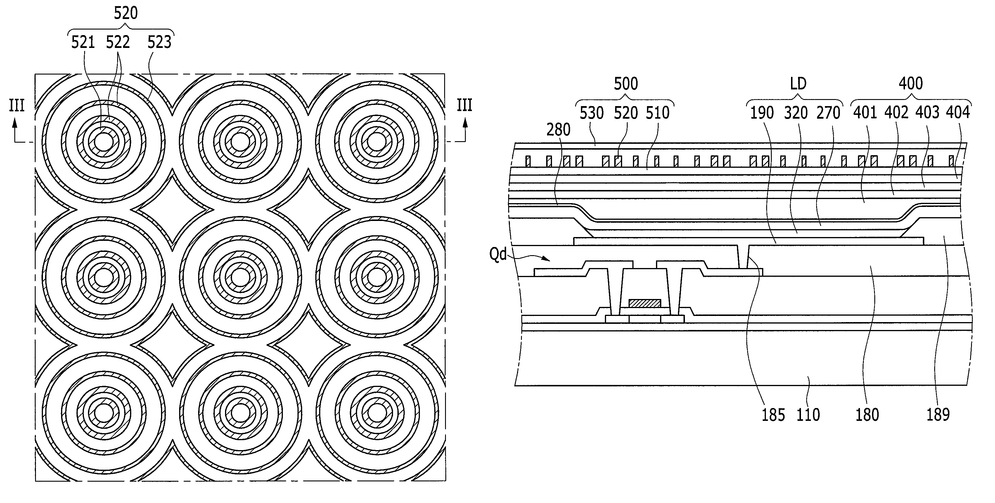
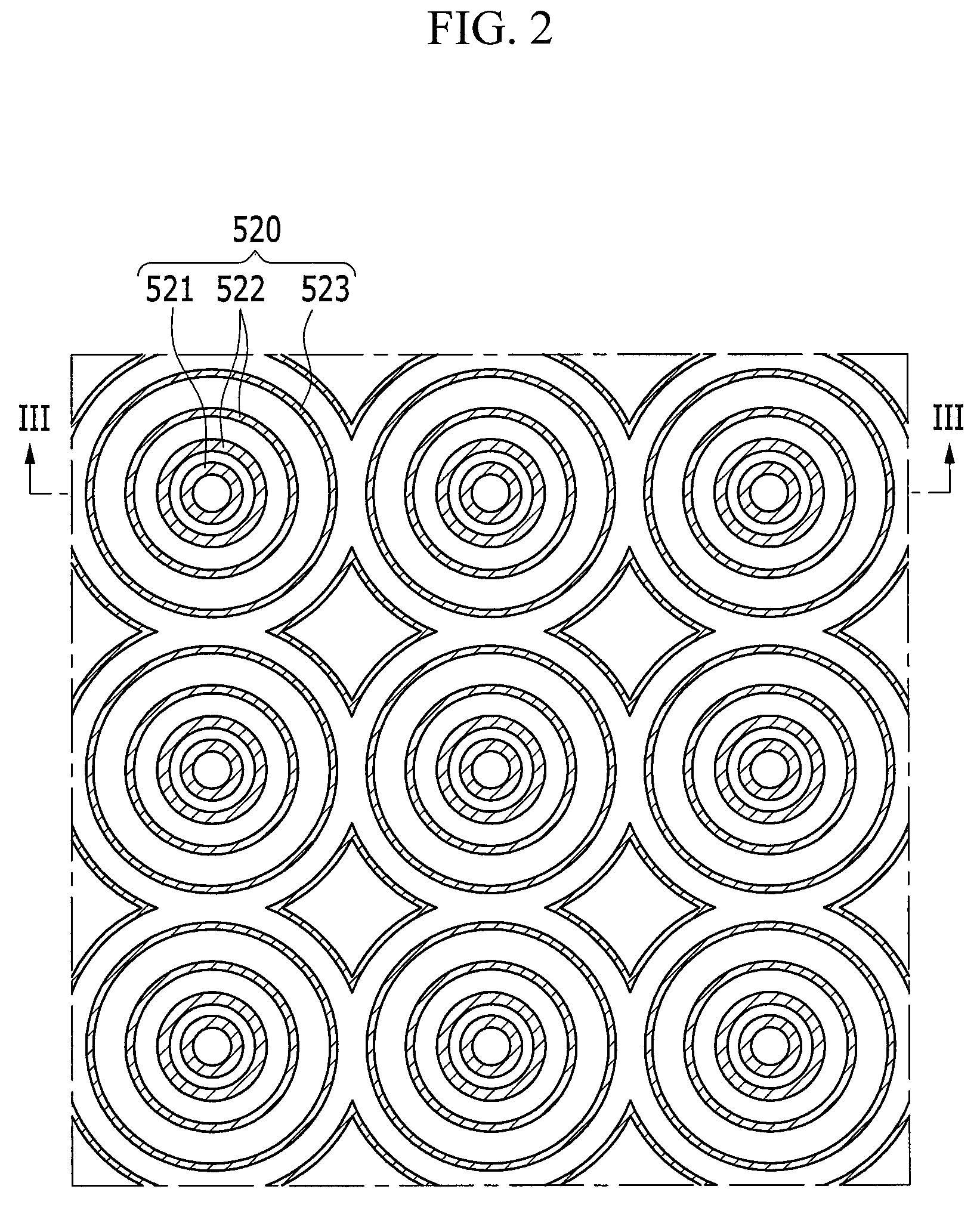
[0040]FIG. 1 is an equivalent circuit schematic drawing of one pixel of an organic light emitting diode (OLED) display according to a first exemplary embodiment.

[0041]Referring to FIG. 1, an organic light emitting device according to the present exemplary embodiment includes a plurality of signal lines 121, 171, and 172, and a pixel PX connected thereto. The pixel PX may be one of a red pixel R, a green pixel G, and a blue pixel B.

[0042]The signal lines include a plurality of scan signal lines 121 for transmitting gate signals (or scanning signals), a plurality of data lines 171 for transmitting data signals, and a plurality of driv...


PUM


Abstract

An organic light emitting diode (OLED) display includes: a substrate; an organic light emitting element on the substrate; a thin film encapsulation layer covering the organic light emitting element; and a viewing angle compensation layer on the thin film encapsulation layer, wherein the viewing angle compensation layer corresponding to a pixel of the organic light emitting element has a plurality of sub-viewing angle compensation members. Accordingly, in the organic light emitting diode (OLED) display according to an exemplary embodiment, the viewing angle compensation layer is disposed on the thin film encapsulation layer such that optical characteristic changes such as the luminance change and the color change according to the viewing angle may be minimized or reduced.

Description

CROSS-REFERENCE TO RELATED APPLICATION[0001]This application claims priority to and the benefit of Korean Patent Application No. 10-2011-0092152 filed in the Korean Intellectual Property Office on Sep. 9, 2011, the entire content of which is incorporated herein by reference.BACKGROUND[0002]1. Field[0003]Aspects of embodiments according to the present invention relate generally to an organic light emitting diode (OLED) display.[0004]2. Description of Related Art[0005]An organic light emitting diode (OLED) display includes organic light emitting elements each formed of a hole injection electrode, an organic emission layer, and an electron injection electrode. With the OLED display, electrons and holes are combined with each other in the organic emission layer to thereby generate excitons. When the excitons shift from the excited state to the ground state, energy is released so as to emit light, and images are displayed on the basis of the emitted light.[0006]An OLED display is a flat ...

Claims


Application Information

Patent Timeline
Patent Type & Authority Patents(United States)
IPC IPC(8): H01J1/62H01J63/04
CPCH05B33/10H01L51/5275H01L2251/5315H01L51/5253H05B33/04H05B33/12H10K50/844H10K50/858H10K2102/3026H05B33/22H10K50/85H10K50/84
Inventor PARK, HYE-JUNGPARK, SOON-RYONGJUNG, WOO-SUKKIM, SUN-HWA
Owner SAMSUNG DISPLAY CO LTD
Why Eureka
Try Eureka