Piezoelectric devices including electrode-less vibrating portions

a piezoelectric device and electrode-less technology, applied in piezoelectric/electrostrictive/magnetostrictive devices, piezoelectric/electrostriction/magnetostriction machines, electrical equipment, etc., can solve problems such as air leakage, vibration interference, and device vibration, and achieve effective hermetic sealing

Inactive Publication Date: 2014-01-07
NIHON DEMPA KOGYO CO LTD
View PDF27 Cites 2 Cited by
  • Summary
  • Abstract
  • Description
  • Claims
  • Application Information

AI Technical Summary

Benefits of technology

[0015]Various embodiments of piezoelectric devices described herein establish a predetermined gap between the piezoelectric vibrating board and each of its excitation “space” electrodes. The embodiments also provide effective hermetic sealing of the packages of the piezoelectric devices using adhesive applied adjacent convexity(ies) surrounding respective excitation electrodes.
[0016]The subject devices are easier than conventional devices to surface-mount because the subject devices provide one or two external electrodes on the outer surface of a respective cover board.

Problems solved by technology

Excitation electrodes formed directly on the main surfaces of the crystal board can adversely affect its vibration.
Even a crystal substrate configured to vibrate at a fundamental frequency of 300 MHz or higher can exhibit vibrational interference caused by the presence of excitation electrodes formed directly on the main surfaces of the crystal substrate.
Consequently, the devices are susceptible to air leaks from outside to inside the package.
These leaks can cause the device to exhibit excessive temporal drift of vibration parameters.
This technique cannot be performed using common solder paste or conventional mounting steps; rather, a special procedure is required.

Method used


Image

  • Piezoelectric devices including electrode-less vibrating portions
  • Piezoelectric devices including electrode-less vibrating portions
  • Piezoelectric devices including electrode-less vibrating portions

Examples


first embodiment

of Method for Manufacturing Piezoelectric Device

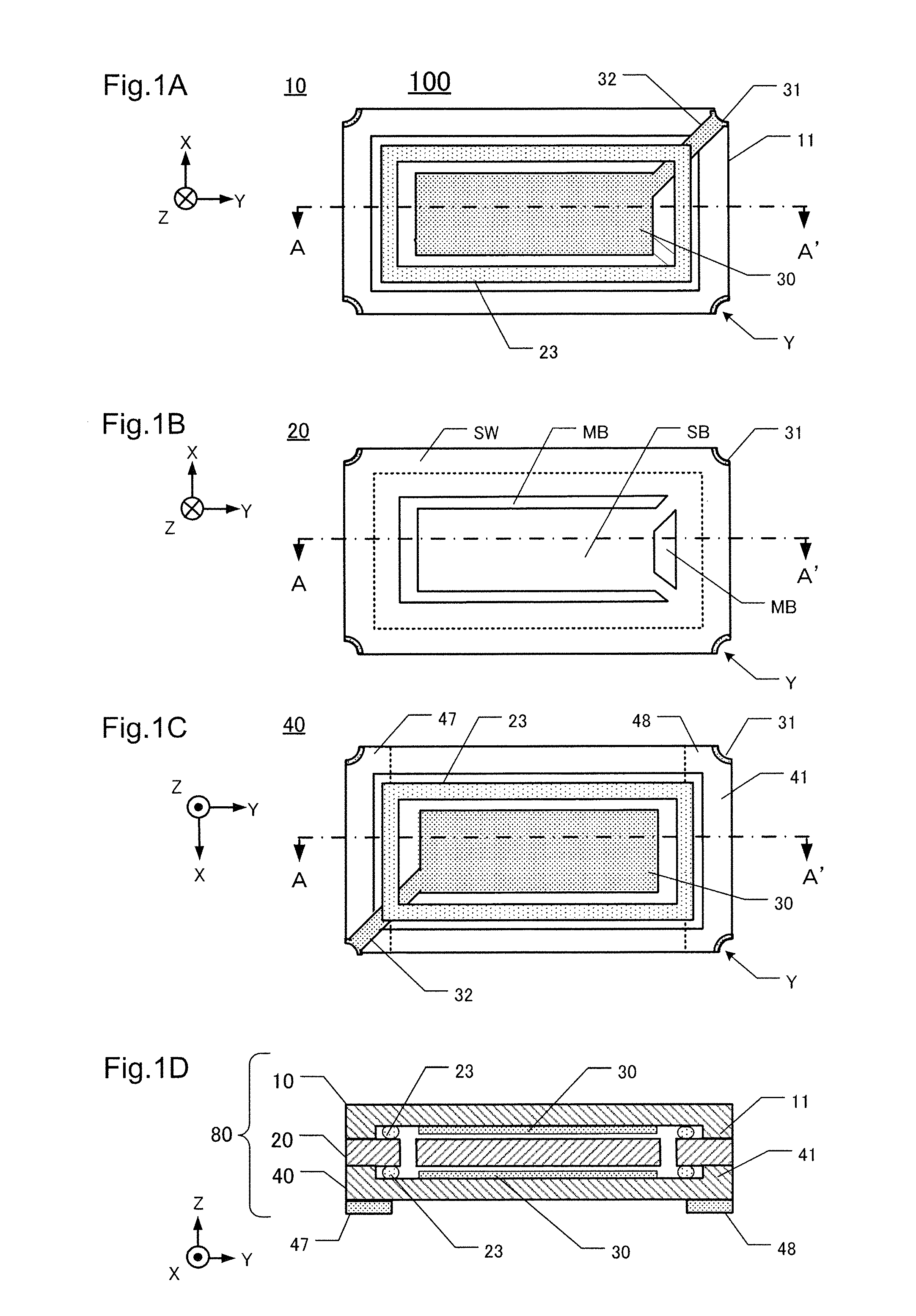
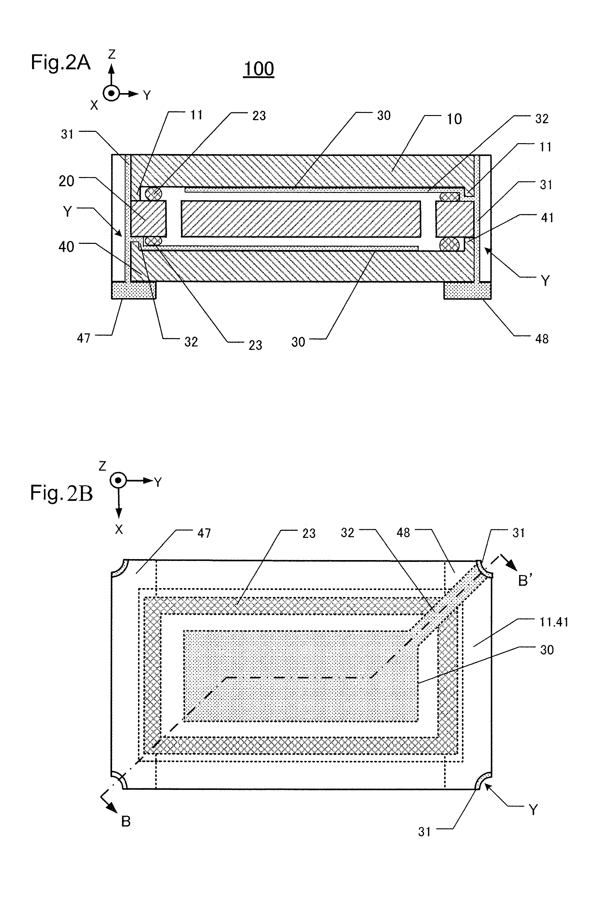
[0056]Multiple second cover boards 40 are typically made simultaneously by forming many of them on a single wafer, called a “second cover wafer 40W.” Similarly, multiple first cover boards 10 are typically made simultaneously by forming many of them on a single wafer, called a “first cover wafer 10W.” Also, similarly, multiple piezoelectric vibrating boards 20 are made simultaneously by forming many of them on a single wafer, called a “crystal wafer”20W.

[0057]FIGS. 3A and 3B are flow-charts of respective portions of this embodiment of a method for manufacturing the piezoelectric device 100. The depicted steps can be performed to manufacture the devices one at a time or to manufacture multiple devices (hundreds to thousands) simultaneously by conducting the process steps on wafers containing multiple individual components.

[0058]In step S102 a convexity 11 is formed in a region (XY plane) of a first cover wafer 10W. The outside edge of t...

second embodiment

of Piezoelectric Device

[0075]FIGS. 6A-6D are schematic views of this embodiment of a piezoelectric device 110 provided with space electrodes and operable by space-voltage impression (induction) to cause vibrations in the piezoelectric vibrating board. FIG. 6A is a plan view of a first cover board 10A as viewed from the piezoelectric vibrating board. FIG. 6B is a plan view of the piezoelectric vibrating board 20 used in this embodiment. FIG. 6C is a plan view of a second cover board 40A as viewed from the piezoelectric vibrating board. FIG. 6D is a cross-sectional view of the piezoelectric device 110 along the line E-E′ in each of FIGS. 6A, 6B, and 6C. Thus, this second embodiment of a piezoelectric device 110 comprises one piezoelectric vibrating board 20, a first cover board 10A, and a second cover board 40A. The cover boards 10A, 40A are made of glass, ceramic, or a crystal material (e.g., quartz crystal).

[0076]In FIG. 6A, the inner main surface of the first cover board 10A includ...

third embodiment

of Piezoelectric Vibrating Device

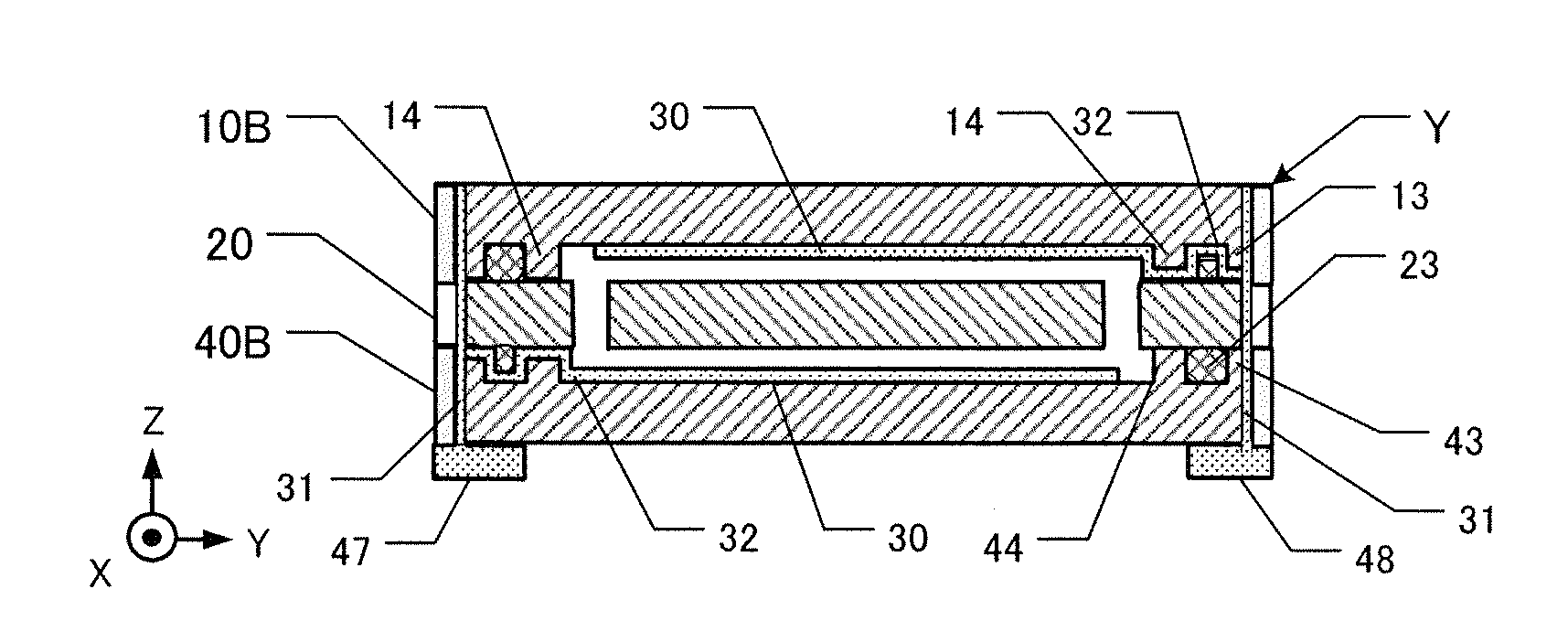
[0082]This embodiment 120 is shown in FIGS. 7A-7D, which are respective schematic views. FIG. 7A is a plan view of a first cover board 10B as viewed from the piezoelectric vibrating board. FIG. 7B is a plan view of the piezoelectric vibrating board 20. FIG. 7C is a plan view of the second cover board 40B. FIG. 7D is a cross-sectional view of the piezoelectric device 120 along the line F-F′ of FIGS. 7A, 7B, and 7C. This embodiment 120 comprises the piezoelectric vibrating board 20, the first cover board 10B, and the second cover board 40B. The first and second cover boards 10B, 40B are made of glass, ceramic, or a crystal material (e.g., quartz crystal).

[0083]As shown in FIG. 7A, the first cover board 10B has a first convexity 13 and a second convexity 14 facing the piezoelectric vibrating board 20. The convexities 13, 14 are made by etching regions other than them, and have equal heights in the Z-direction. The first convexity 13 is just inboard of t...


PUM


Abstract

An exemplary piezoelectric device has a piezoelectric vibrating board including a portion that exhibits thickness-shear vibration, and a frame portion extending around and supporting the vibrating portion. A first cover board, bonded to the first main surface of the frame portion, has a first excitation electrode. A second cover board, bonded to the second main surface of the frame portion, has a second excitation electrode. Thus, the vibrating portion is sealed in a package formed by the frame portion and cover boards. A first convexity, defined either on the bonded main surface of the first cover board or on the first main surface of the frame portion, surrounds the excitation electrode and establishes a predetermined gap between the vibrating portion and excitation electrode. The first cover board and frame portion are bonded by adhesive applied, adjacent the first convexity but not on the first convexity, continuously around the vibrating portion.

Description

CROSS-REFERENCE TO RELATED APPLICATION[0001]This application claims priority to and the benefit of Japan Patent Application No. 2010-069131, filed on Mar. 25, 2010 in the Japan Patent Office, the disclosure of which is incorporated herein by reference in its entirety.FIELD[0002]This disclosure pertains to, inter alia, surface-mount type piezoelectric devices.DESCRIPTION OF THE RELATED ART[0003]One conventional type of “piezoelectric device” includes a “board” (substrate) of AT-cut quartz crystal enclosed in a “package.” The crystal board has upper and lower main surfaces on which respective excitation electrodes have been formed. When electrically excited via the excitation electrodes, the AT-cut crystal exhibits “thickness shear” vibration. The fundamental resonance frequency at which the AT-cut crystal substrate vibrates is a function of substrate thickness (between the upper and lower main surfaces), wherein the frequency varies inversely with substrate thickness.[0004]Excitation...

Claims


Application Information

Patent Timeline
Patent Type & Authority Patents(United States)
IPC IPC(8): H01L41/053
CPCH03H9/02H03H9/1035H03H9/19
Inventor TAKAHASHI, TAKEHIRO
Owner NIHON DEMPA KOGYO CO LTD
Why Eureka
Try Eureka