Multi-junction PV module

a photovoltaic device and multi-junction technology, applied in the direction of pv power plants, sustainable manufacturing/processing, final product manufacturing, etc., can solve the problems of reducing affecting the efficiency of the device, and limiting the conversion efficiency of solar power into electricity of the device to a maximum of about 37%, so as to achieve high current protection diodes

Active Publication Date: 2014-09-16
SUNLIGHT PHOTONICS
View PDF64 Cites 92 Cited by
  • Summary
  • Abstract
  • Description
  • Claims
  • Application Information

AI Technical Summary

Problems solved by technology

The conversion efficiency of solar power into electricity of this device is limited to a maximum of about 37%, since photon energy in excess of the semiconductor's bandgap is wasted as heat.
This current-matching procedure complicates the design and decreases the efficiency of the device.
If a part of the solar spectrum is absorbed or scattered, e.g. by water vapors, the resulting disproportional decrease of photocurrent in one of junctions will limit the current through the whole device and thus decrease its conversion efficiency.

Method used


Image

  • Multi-junction PV module
  • Multi-junction PV module
  • Multi-junction PV module

Examples


examples

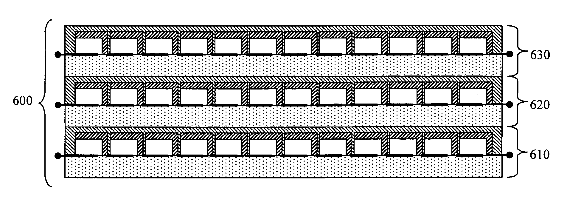
[0065]In one embodiment of this invention, a two junction layer PV module may be produced as shown in FIG. 8. Bottom junction layer 810 may be made of several thin-film cells 812, which are monolithically integrated and connected electrically in series to form a single string. Corresponding thin-film semiconductor absorber material may be based on CuInSe2 compound and its alloys with Ga and S, more commonly known in the industry as CIGS. Similarly, top junction layer 820 may be also made of several CIGS-based cells 822, which are monolithically integrated and connected electrically in series into a single string. It may be preferred to adjust the CIGS compositions of cells 812 and 822 so that their respective optical bandgaps are about 1.1 eV and 1.7 eV. The respective compositions of cells 812 and 822 in this case may be close to CuIn0.8Ga0.2Se2 and CuGaSe2, for instance. Monolithic integration of these CIGS cells may be accomplished by laser and mechanical scribing. The top juncti...


PUM


Abstract

A photovoltaic device is provided which includes a plurality of junction layers. Each junction layer includes a plurality of photovoltaic cells electrically connected to one another. At least one of the junction layers is at least in part optically transmissive. The junction layers are arranged in a stack on top of each other.

Description

BACKGROUND[0001]1. Field[0002]The present invention relates generally to a method of manufacturing thin-film photovoltaic devices, and particularly to a method for the manufacturing of high-efficiency thin-film photovoltaic devices.[0003]2. Related Art[0004]Photovoltaic devices represent one of the major sources of environmentally clean and renewable energy. They are frequently used to convert optical energy into electrical energy. Typically, a photovoltaic device is made of one semiconducting material with p-doped and n-doped regions. The conversion efficiency of solar power into electricity of this device is limited to a maximum of about 37%, since photon energy in excess of the semiconductor's bandgap is wasted as heat. A photovoltaic device with multiple semiconductor layers of different bandgaps is more efficient: an optimized two-bandgap photovoltaic device has the maximum solar conversion efficiency of 50%, whereas a three-bandgap photovoltaic device has the maximum solar con...

Claims


Application Information

Patent Timeline
Patent Type & Authority Patents(United States)
IPC IPC(8): H01L31/042H01L25/04H01L27/142H01L31/048
CPCH01L31/042H01L31/0485H01L25/045H01L27/1423Y02E10/50H01L31/0504H01L31/043H01L31/046H01L31/0687H02S40/34Y02E10/544Y02P70/50
Inventor FROLOV, SERGEYBRUCE, ALLAN JAMESCYRUS, MICHAEL
Owner SUNLIGHT PHOTONICS
Why Eureka
Try Eureka