
Methods for forming electrically precise capacitors, and structures formed therefrom

a technology of precise capacitors and capacitors, which is applied in the manufacture of capacitors, semiconductor/solid-state devices, fixed capacitor details, etc., can solve the problems of poor level, poor conformality, and difficulty in precisely forming insulating layers, and achieve precise and conformal capacitors. , the effect of higher conformality

Inactive Publication Date: 2015-03-10
ENSURGE MICROPOWER ASA
View PDF16 Cites 2 Cited by
  • Summary
  • Abstract
  • Description
  • Claims
  • Application Information

AI Technical Summary

Benefits of technology

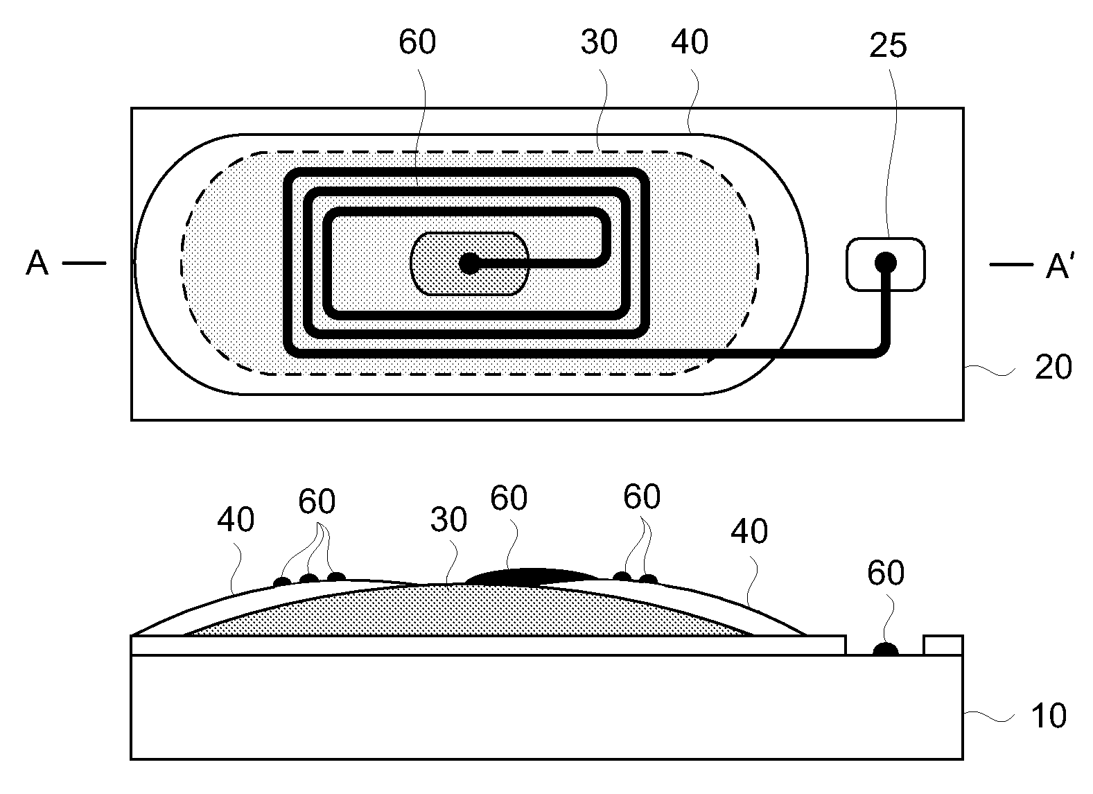
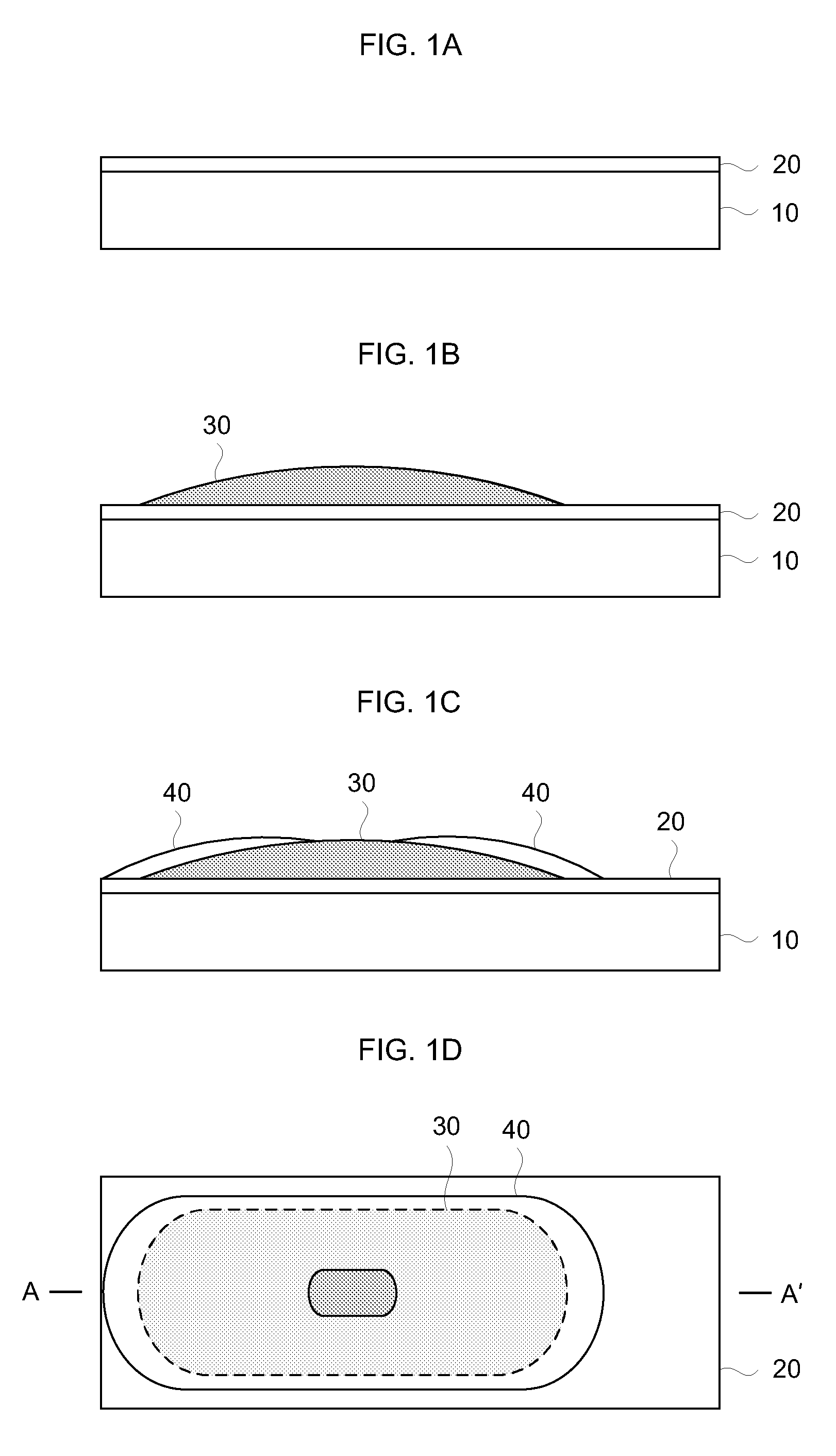
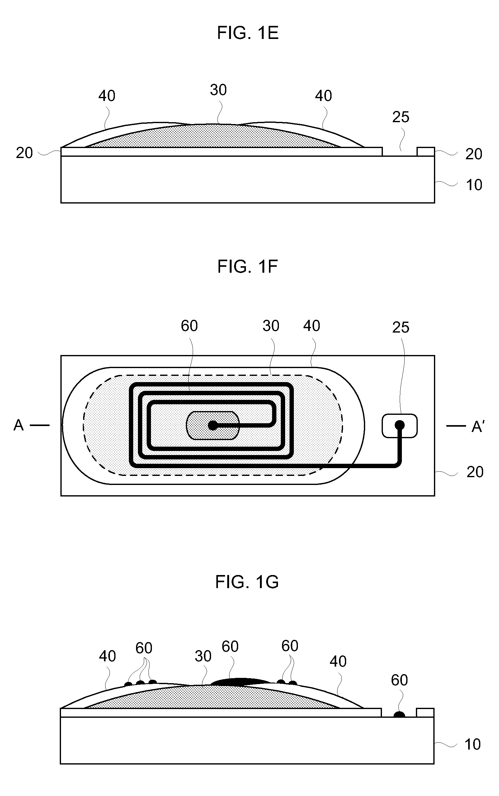
[0005]The present invention is directed to methods of making thin film devices (e.g., transistors, capacitors, diodes, etc.) and circuits including the same on various substrates including, but not limited to, glass (e.g., silica, quartz) sheets, wafers or slips, plastic and / or metal foils or sheets, silicon wafers, etc., all of which may carry one or more additional (e.g., buffer, planarization mechanical support, etc.) layers. More specifically, embodiments of the present invention relate to an improved deposition process (e.g., atomic layer deposition) for forming an insulating layer on the substrate. Atomic layer deposition (ALD) of the insulating layer provides a higher level of conformality of the insulating layer over the substrate. Thus, the processes described herein allow for a more precise and conformal capacitor in dielectric high performance printed electronic devices, such as wireless circuits, RFID and other identification tags, EAS devices, etc.
[0010]Embodiments of the present invention enable precise deposition of an insulating layer on substrates of various surface roughnesses and compositions. In addition, the present invention advantageously utilizes atomic layer deposition (ALD) for depositing an insulating layer on a substrate without the need for additional planarization through high cost polishing of the substrate surface. A further aspect of the present invention replaces the relatively difficult-to-control conventional processes and structures, by providing a deposition process that produces a high level of conformality in the insulating layer on a wide range of substrates.
[0011]Embodiments of the present invention may eliminate thin spots or undeposited areas in capacitor dielectric, which may lead to premature breakdown and / or high defect densities. Embodiments of the present invention also reduce or eliminate charge leakage and unpredictability in capacitor properties, thereby enabling lower processing margins. Furthermore, embodiments of the present invention eliminate problems with EAS devices that are presumed to be active, but are actually inactive or ineffective, or that can be easily deactivated by weak electrical fields. As a result, the present invention provides a more viable production process for making high precision capacitors.

Problems solved by technology

Previously, there have been challenges in precisely depositing an insulating layer on substrates of various surface roughnesses.
Conventional deposition processes have resulted in poor levels of conformality (uniform thickness or surface coverage uniformity of the insulating layer over the substrate) and thickness control, resulting in thin spots or undeposited areas.
Generally, the resulting thin spots or undeposited areas lead to premature breakdown and / or a high defect density in the production of an electronic device.
Thus, an ideal deposition process for depositing insulating layers on substrates having various surface roughnesses has been difficult to achieve.
However, CVD methods may not achieve a desired level of conformality, resulting in the production of substandard capacitors having thin spots or undeposited areas.

Method used


Image

  • Methods for forming electrically precise capacitors, and structures formed therefrom
  • Methods for forming electrically precise capacitors, and structures formed therefrom
  • Methods for forming electrically precise capacitors, and structures formed therefrom

Examples


Embodiment Construction

[0022]Reference will now be made in detail to preferred embodiments of the invention, examples of which are illustrated in the accompanying drawings. While the invention will be described in conjunction with preferred embodiments, it will be understood that they are not intended to limit the invention to these embodiments. On the contrary, the invention is intended to cover alternatives, modifications and equivalents that may be included within the spirit and scope of the invention as defined by the appended claims. Furthermore, in the following detailed description of the present invention, numerous specific details are set forth in order to provide a thorough understanding of the present invention. However, it will be readily apparent to one skilled in the art that the present invention may be practiced without these specific details. In other instances, well-known methods, procedures, components, and circuits have not been described in detail so as not to unnecessarily obscure as...


PUM

PropertyMeasurementUnit
thicknessaaaaaaaaaa
radiusaaaaaaaaaa
radiusaaaaaaaaaa

Abstract

High precision capacitors and methods for forming the same utilizing a precise and highly conformal deposition process for depositing an insulating layer on substrates of various roughness and composition are disclosed. The method generally includes the steps of depositing a first insulating layer on a metal substrate by atomic layer deposition (ALD); (b) forming a first capacitor electrode on the first insulating layer; and (c) forming a second insulating layer on the first insulating layer and on or adjacent to the first capacitor electrode. The methods provide an improved deposition process that produces a highly conformal insulating layer on a wide range of substrates, and thereby, an improved capacitor.

Description

RELATED APPLICATIONS[0001]This application is a divisional of U.S. patent application Ser. No. 12 / 249,841, filed Oct. 10, 2008, which claims the benefit of U.S. Provisional Application No. 60 / 979,054, filed Oct. 10, 2007, each of which is incorporated herein by reference in its entirety.FIELD OF THE INVENTION[0002]Embodiments of the present invention relate to depositing (e.g., by atomic layer deposition) or otherwise forming a uniform, highly conformal insulating layer to form a high precision capacitor. Embodiments of the present invention provide improved control of the insulating layer deposition process on various substrates of various surface roughnesses, allowing for more precise insulating layers and processes for making capacitors. As a result, high precision capacitors can be formed on a wide range of substrates.DISCUSSION OF THE BACKGROUND[0003]Previously, there have been challenges in precisely depositing an insulating layer on substrates of various surface roughnesses. ...

Claims


Application Information

Patent Timeline
Patent Type & Authority Patents(United States)
IPC IPC(8): H01G4/06H01G4/01H01G13/00
CPCH01G4/01H01G13/00H01G4/005H01G4/33H01G4/002H01L27/016H01L28/60Y10T29/43Y10T29/435Y10T29/49002Y10T29/49016H01G4/10H01G4/30H01Q1/22H01G4/008H01G4/1209H01G4/224H01G4/306H01G4/40H01L23/66H01L2223/6677H01Q1/2283H01Q1/38
Inventor KAMATH, ARVINDCHOI, CRISWELLSMITH, PATRICKSCHER, ERIKLI, JIANG
Owner ENSURGE MICROPOWER ASA
Learn More