Lighting device with built-in RF antenna

a technology of rf antenna and light source, which is applied in the direction of semiconductor devices for light sources, lighting and heating apparatus, light source combinations, etc., to achieve the effect of removing the unavoidable heat dissipation of light sources and wide spatial range of wireless rf communication

Active Publication Date: 2015-11-10
KONINK PHILIPS ELECTRONICS NV
View PDF19 Cites 21 Cited by
  • Summary
  • Abstract
  • Description
  • Claims
  • Application Information

AI Technical Summary

Benefits of technology

[0013]Metallic components of the lighting device having an extension larger than 1 / 10 of a wavelength of the Radio Frequency signals may be arranged at least 4 mm below the virtual plane drawn orthogonal to the optical axis and going through the antenna. Hereby, a very wide RF communication angle can be obtained. Especially, the antenna may be arranged at least 2 mm in front of the heat sink, such as 4 mm in front of the heat sink, thus allowing a wide RF communication angle while enabling the heat sink to be large enough to ensure effective cooling. Metallic components of the lighting device having an extension larger than 1 / 15 of a wavelength, such as larger than 1 / 20, of the Radio Frequency signals are preferably arranged below a virtual plane drawn orthogonal to the optical axis and going through the antenna. Very small metal objects, i.e. small compared to the RF signal wavelength, can be tolerated, e.g. in the form of parts of electronic chips and solder material and the like, while especially the heat sink and such large metallic components significantly destroys RF communication to / from the antenna. Especially, the heat sink may form part of the outer enclosure, such as a significant part of the outer enclosure.
[0016]Alternatively, or additionally, the antenna is disposed on a first Printed Circuit Board (PCB), such as disposed on an end part of the PCB. Hereby, a very compact antenna can be provided, since a PCB will normally be present in the lighting device to hold the necessary electronic circuits for controlling the light source. Especially, the antenna may be disposed on an end part of the first PCB, wherein this end part is arranged for position in an opening of a second PCB, preferably such that the first and second PCBs re substantially perpendicular to each other, and preferably arranged such that the second PCB is substantially perpendicular to the optical axis. The RF communication circuit may be disposed on the first PCB, preferably comprising a matching circuit connected between the antenna and the RF communication circuit. Hereby, a very compact design can be provided, since the first PCB is utilized for a plurality of purposes, and a short distance between the RF circuit and the antenna can be provided, and still further, such PCB is suited for automated manufacturing due to the absence of wiring between antenna and RF circuit. Especially, the RF communication circuit may be disposed on one side of the first PCB, while the antenna is disposed on an opposite side of the first PCB.
[0019]The lighting device may comprise a second antenna, wherein the first and second antennas are oriented so as to radiate RF signals in different directions, such as the first and second antennas being different types of antennas. Hereby an improved compatibility and improved spatial communication range is possible. Especially, the first and second antennas are connected so as to provide antenna diversity.
[0026]In a fourth aspect, the invention provides a method for arranging a Radio Frequency communication antenna within an outer enclosure of a lighting device, such as a replacement lighting device, comprising a light source defining an optical axis, the method comprising arranging the antenna such within the outer enclosure, that metallic components of the lighting device having an extension larger than 1 / 10 of a wavelength of the Radio Frequency signals are arranged below a virtual plane drawn orthogonal to the optical axis and going through the antenna, such that the antenna radiation pattern is not affected significantly.

Problems solved by technology

This is a problem to obtain within the limited dimensions of the outer enclosure of such device, since such dimensions are often dictated by standard size housings and power sockets.

Method used


Image

  • Lighting device with built-in RF antenna
  • Lighting device with built-in RF antenna
  • Lighting device with built-in RF antenna

Examples


Embodiment Construction

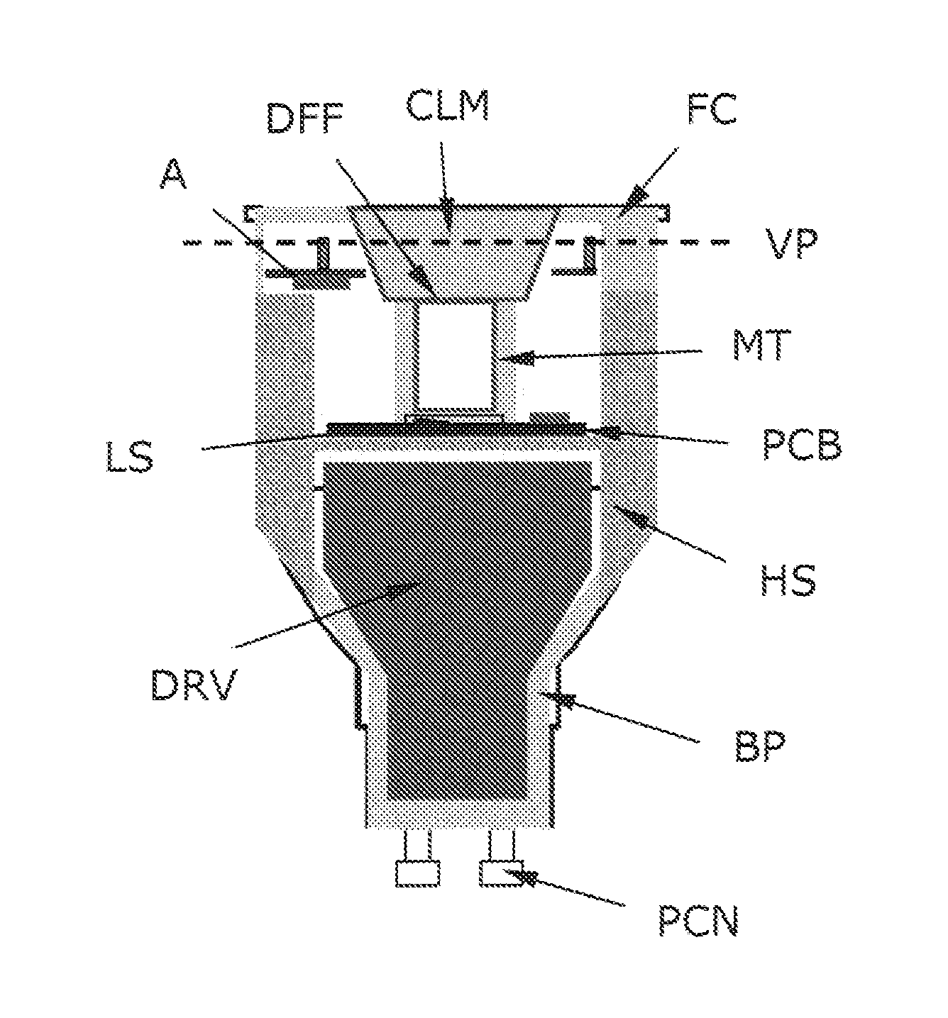
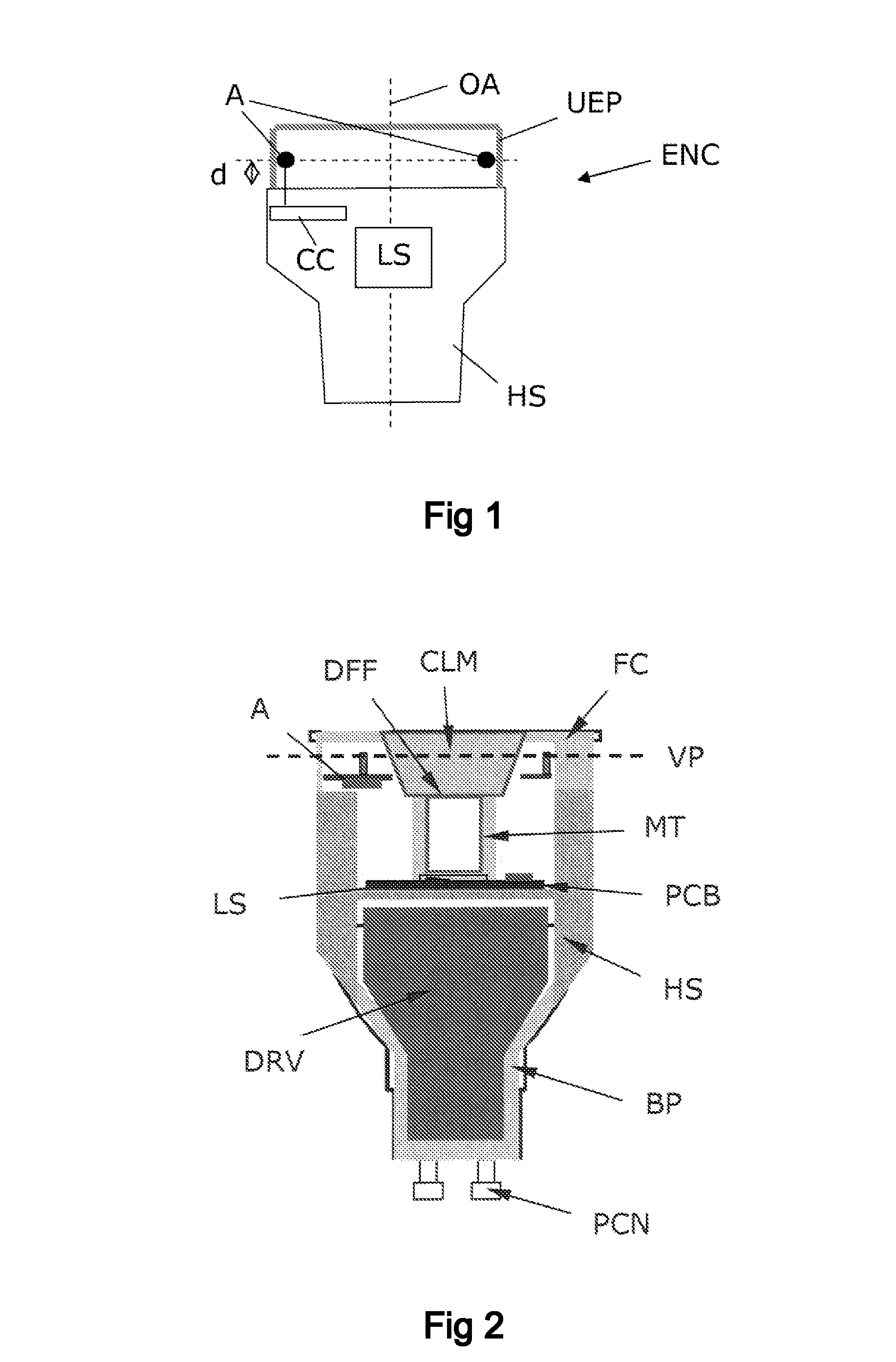
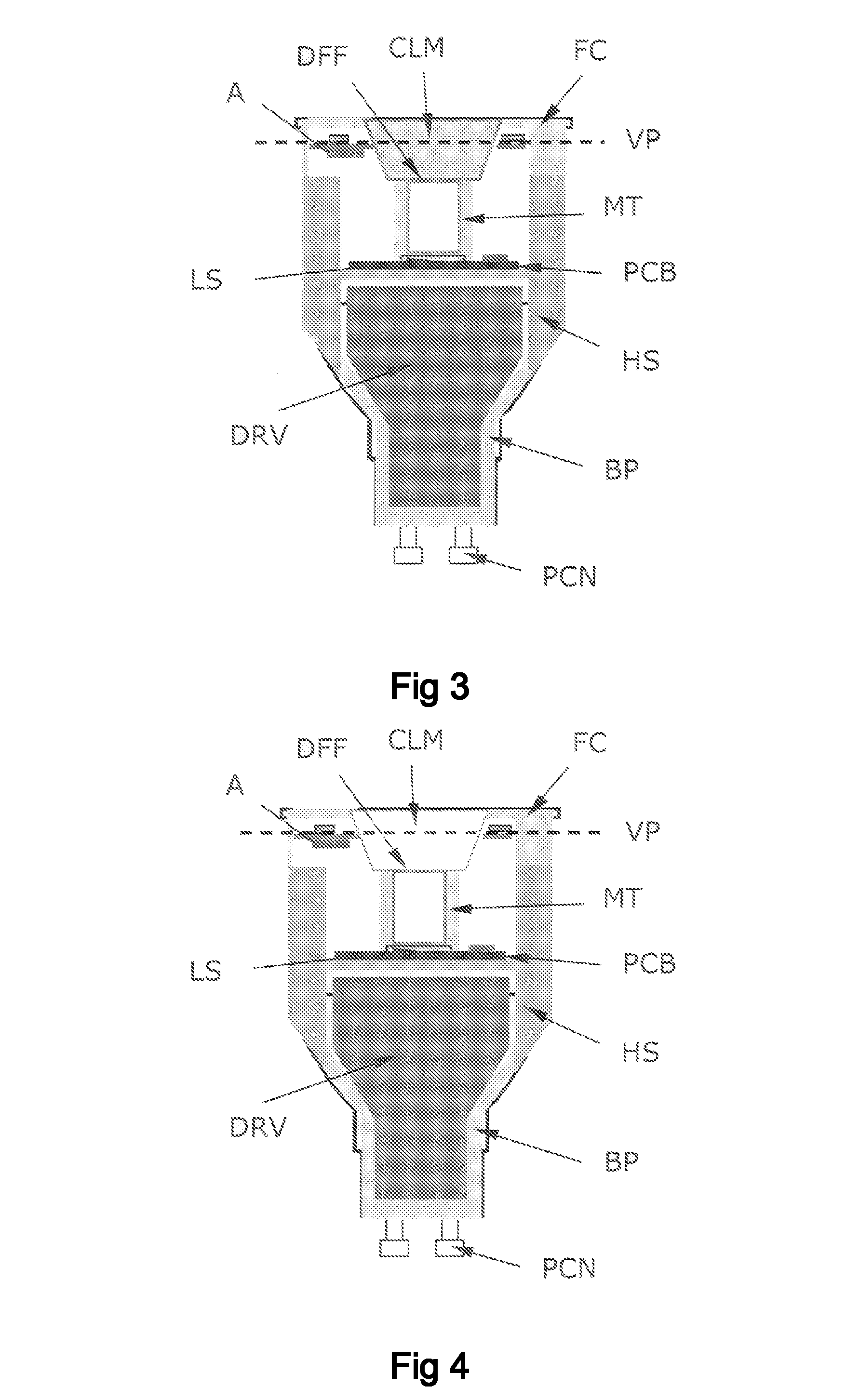
[0035]FIG. 1 illustrates a simple sketch of a section through a lighting device embodiment with an outer enclosure ENC in the form of an upper and a lower part, wherein the lower part is a metal housing HS and the upper part UEP is a non-metallic material, e.g. a polymeric material. The metal housing HS serves as heat sink to transport heat away from the light source LS positioned within the enclosure ENC. The light source LS generates light along an optical axis OA, and the light escapes the outer enclosure ENC through a transparent or translucent part of the upper enclosure part UEP. An RF antenna A in the form of a wire antenna is indicated with black color, and the antenna A is connected to an RF communication circuit CC placed within the outer enclosure ENC. As seen, the antenna A is positioned in the upper enclosure part UEP, i.e. above the metal housing HS. The antenna is placed with a distance d between the metal housing HS and a plane through a plane extended by the antenna...


PUM


Abstract

A lighting device, such as a replacement lighting device, comprising a light source (LS), e.g. LEDs, for producing light along an optical axis (OA). A heat sink (HS) made of a material with an electrical resistivity being less than 0.01 Ωm, e.g. a metallic heat sink being a part of the housing, transports heat away from the light source (LS). A Radio Frequency (RF) communication circuit (CC) connected to an antenna (A) serves to enable RF signal communication, e.g. to control the device via a remote control. Metallic components, including the heat sink (HS), having an extension larger than 1 / 10 of a wavelength of the RF signal are arranged below a virtual plane (VP) drawn orthogonal to the optical axis (OA) and going through the antenna (A). Hereby a compact device can be obtained, and still a satisfying RF radiation pattern can be obtained. The antenna can be a wire antenna or a PCB antenna, e.g. a PIFA or a IFA type antenna. In a special embodiment the antenna is formed on a ring-shaped PCB with a central hole allowing passage of light from the light source. Preferably, the antenna is positioned at least 2 mm in front of the heat sink (HS).

Description

FIELD OF THE INVENTION[0001]The present invention relates to the field of lighting devices. More specifically, the invention provides a lighting device, e.g. in the form of a standard power socket lamp, with a built-in Radio Frequency (RF) antenna. The invention provides a lighting device with an antenna suited for reliable communication of RF signals in a wide directivity pattern.BACKGROUND OF THE INVENTION[0002]Intelligent lighting has become widespread, and RF communication is a powerful technology to be used in the tele management of lamps, in particular for domestic and office environments. Instead of controlling the power, e.g. 230 V supply, to the lamp, the trend has moved towards directly controlling the light source or lighting device, i.e. the exchangeable element of the lamp, by sending an RF control signal to the lighting device. For indoor use the ISM band covers suitable frequencies to allow communication over a range of up to 20 meter. A suitable communication standar...

Claims


Application Information

Patent Timeline
Patent Type & Authority Patents(United States)
IPC IPC(8): H01Q1/26H01Q3/36H01Q1/52H01Q1/38H01Q1/44H01Q9/42H05B33/08H05B37/02F21V23/04F21K99/00F21V3/00F21V29/85F21Y101/02F21Y113/00H05B44/00
CPCH01Q1/44F21V23/045F21V23/0435H01Q1/38H01Q1/52H01Q3/36H01Q9/42H05B33/0803H05B33/0845H05B37/0272F21K9/135F21K9/137F21V3/00F21V29/85F21Y2101/02F21Y2113/005F21K9/232F21K9/233F21Y2115/10F21Y2113/13H05B45/00H05B45/10H05B47/19H05B45/357
Inventor CHEN, BINGZHOUZHANG, GUOPINGLANKHORST, MARTIJN HENRI RICHARDDENKER, ROGER HENRISNELTEN, JEROENCLAESSENS, DENNIS JOHANNES ANTONIUSHAENEN, LUDOSELEN, JACOBUS HUBERTUS ANNAVAN KOOTEN, PATRICK
Owner KONINK PHILIPS ELECTRONICS NV
Why Eureka
Try Eureka