Integrated circuit with sensor and method of manufacturing such an integrated circuit

a technology of integrated circuits and sensors, applied in semiconductor/solid-state device testing/measurement, semiconductor/solid-state device details, coatings, etc., can solve problems such as interference with the correct operation of the underlying circuit elements of the ic, risk of moisture entering the metallization stack, and communication between environmental sensors

Active Publication Date: 2016-03-15
SCIOSENSE BV
View PDF21 Cites 3 Cited by
  • Summary
  • Abstract
  • Description
  • Claims
  • Application Information

AI Technical Summary

Benefits of technology

[0007]It is particularly attractive to integrate at least some of these sensors in the back-end of the manufacturing process of an IC, such as in the metallization stack, as this facilitates a cost-effective route to such integration due to the fact that such integration can be achieved with minimal alteration to the process flow.
[0028]Alternatively, the method further comprises forming a further via in said opening and forming a bond pad on the passivation stack that is conductively coupled to the further via such that the passivation stack does not require a permanent opening to provide access to the bond pad.

Problems solved by technology

However, one of the challenges IC designers are faced with when integrating multiple sensors into the metallization stack is that environmental sensors have to be in communicative contact with the environment.
This increases the risk that moisture penetrates the metallization stack and interferes with the correct operation of the underlying circuit elements of the IC.
Unfortunately, when integrating multiple sensors with different functionality in the metallization layer, the partial removal of such a barrier layer cannot always be avoided.
This is of course unwanted as such moisture penetration can detrimentally affect the operation of the IC as previously explained.
However, the integration of moisture-sensitive sensors is not without problems, as it proves difficult to protect the other circuitry of the IC from exposure to moisture, at least in a cost-effective manner.

Method used


Image

  • Integrated circuit with sensor and method of manufacturing such an integrated circuit
  • Integrated circuit with sensor and method of manufacturing such an integrated circuit
  • Integrated circuit with sensor and method of manufacturing such an integrated circuit

Examples


Embodiment Construction

[0029]Embodiments of the invention are described in more detail and by way of non-limiting examples with reference to the accompanying drawings, wherein:

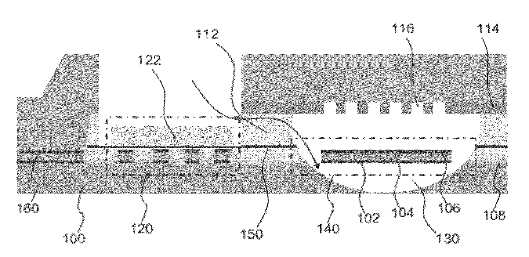
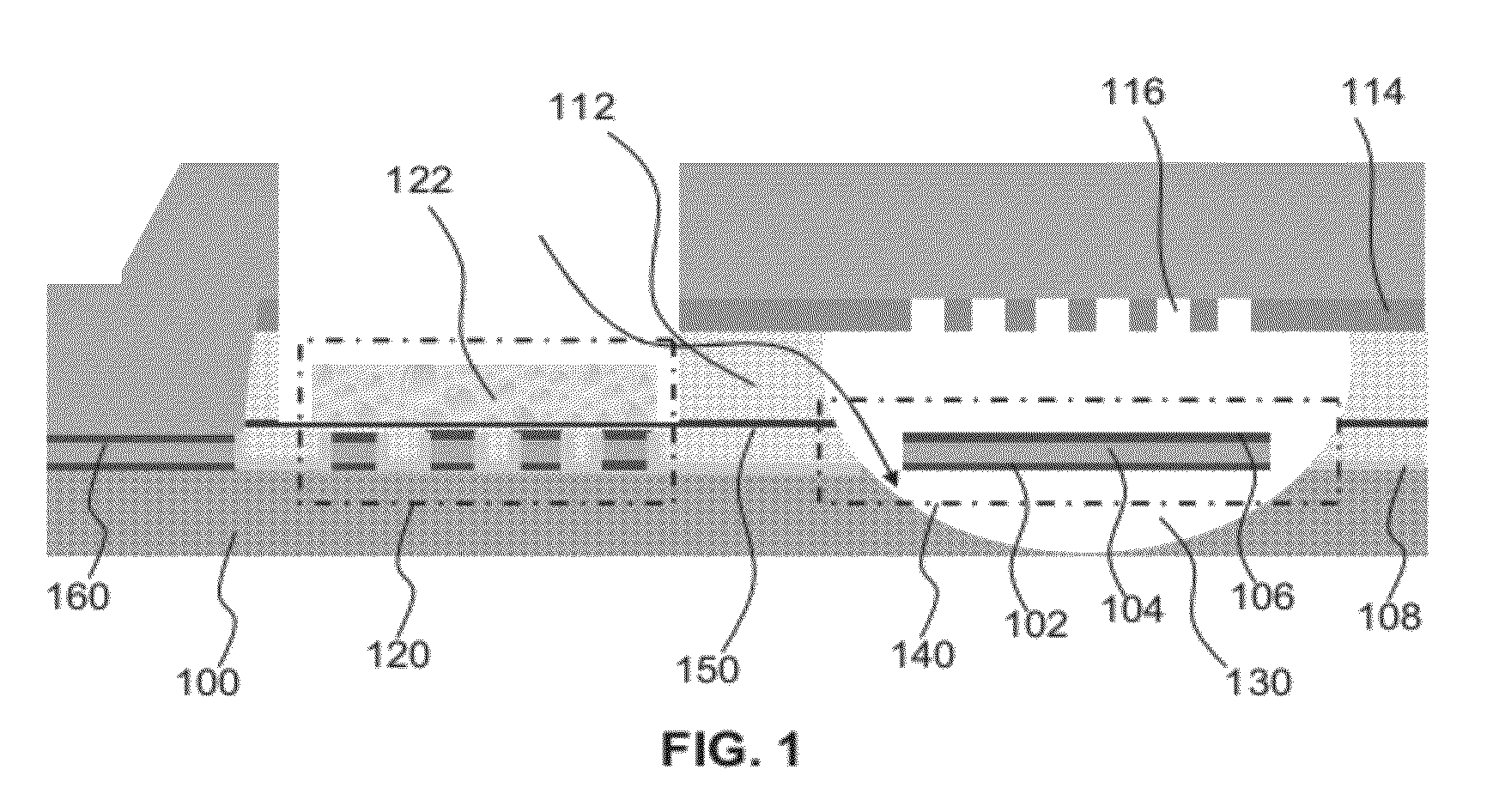
[0030]FIG. 1 schematically depicts a prior art IC with multiple sensors;

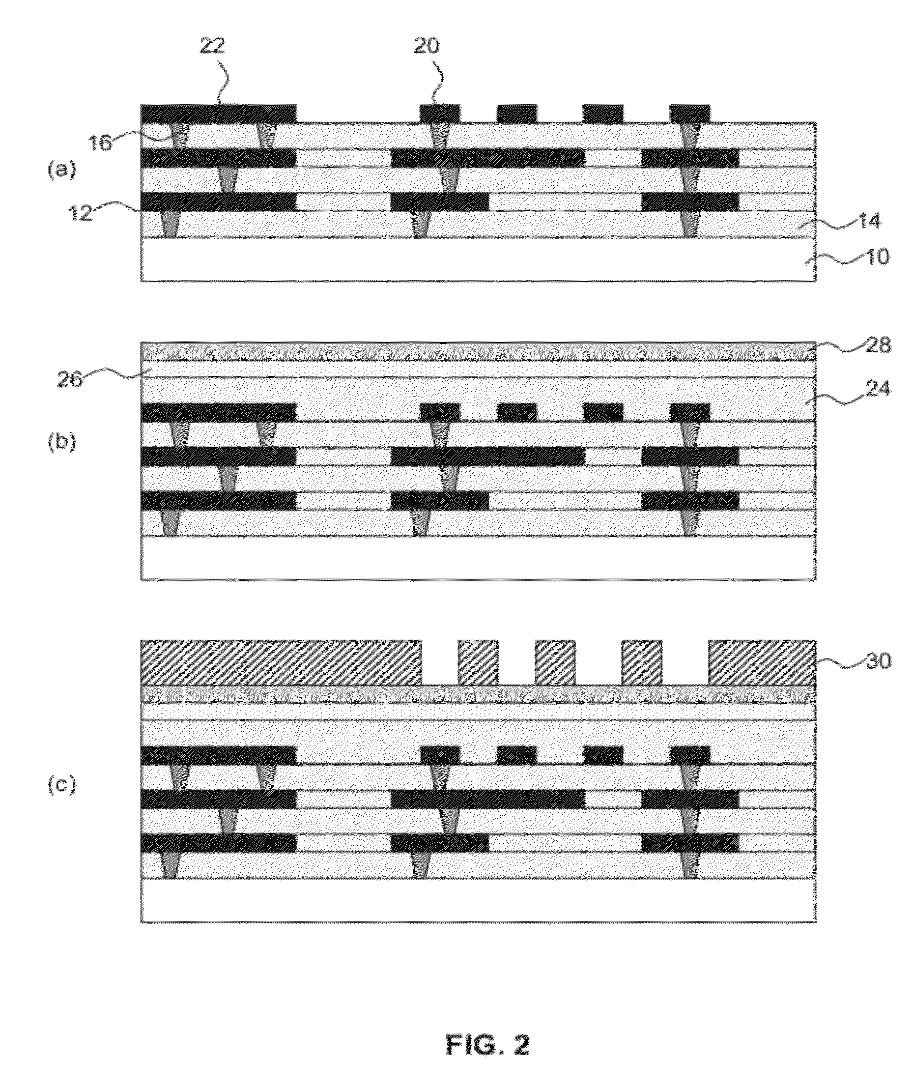
[0031]FIG. 2 schematically depicts a method to manufacture an IC with a sensor in accordance with an embodiment of the present invention;

[0032]FIG. 3 schematically an IC with a sensor in accordance with another embodiment of the present invention;

[0033]FIG. 4 schematically depicts a method to manufacture an IC with a sensor in accordance with yet another embodiment of the present invention;

[0034]FIG. 5 schematically depicts a method to manufacture an IC with a sensor in accordance with yet another embodiment of the present invention;

[0035]FIG. 6 schematically depicts an IC with a sensor in accordance with yet another embodiment of the present invention; and

[0036]FIG. 7 schematically depicts an IC with a sensor in accordance with yet another embodiment of the pre...


PUM

PropertyMeasurementUnit
thicknessaaaaaaaaaa
dielectric constantaaaaaaaaaa
relative humidityaaaaaaaaaa

Abstract

Disclosed is an integrated circuit comprising a substrate (10) carrying a plurality of circuit elements; a metallization stack (12, 14, 16) interconnecting said circuit elements, said metallization stack comprising a patterned upper metallization layer comprising a first metal portion (20); a passivation stack (24, 26, 28) covering the metallization stack; and a sensor including a sensing material (40) on the passivation stack, said sensor being coupled to the first metal portion by a via (34) extending through the passivation stack. A method of manufacturing such an IC is also disclosed.

Description

CROSS-REFERENCE TO RELATED APPLICATIONS[0001]This application claims the priority under 35 U.S.C. §119 of European patent application no. 11155468.9, filed on Feb. 22, 2011, the contents of which are incorporated by reference herein.[0002]The present invention relates to an integrated circuit (IC) comprising a substrate carrying a plurality of circuit elements; a metallization stack interconnecting said circuit elements, said metallization stack comprising a patterned upper metallization layer comprising a first metal portion; a passivation stack covering the metallization stack; and a sensor.[0003]The present invention further relates to a method of manufacturing such an IC.[0004]Nowadays, integrated circuits (ICs) may comprise moisture-sensitive sensors, such as relative humidity (RH) sensors or liquid immersion detection sensors. Such sensors may be included in the IC design for a number of reasons.[0005]For instance, such a sensor may be included in the ICs to determine whether ...

Claims


Application Information

Patent Timeline
Patent Type & Authority Patents(United States)
IPC IPC(8): H01L29/66B81C1/00
CPCB81C1/00246B81C2203/0714H01L2924/0002H01L2924/00H01L21/4853H01L21/56H01L22/34H01L23/3192H01L23/49811H01L23/564
Inventor DAAMEN, ROELWOLTERS, ROBERTUS ADRIANUS MARIARONGEN, RENE THEODORA HUBERTUSPONOMAREV, YOURI VICTOROVITCH
Owner SCIOSENSE BV
Why Eureka
Try Eureka