

Radiation imaging apparatus and radiation imaging system
a radiation imaging and radiation imaging technology, applied in the field of radiation imaging apparatus and radiation imaging system, can solve the problem of not accurately detecting the signals output from the pixels for radiation detection, and achieve the effect of accurately monitoring radiation independently
- Summary
- Abstract
- Description
- Claims
- Application Information
AI Technical Summary
Benefits of technology
Problems solved by technology
Method used
Image

Examples
first embodiment
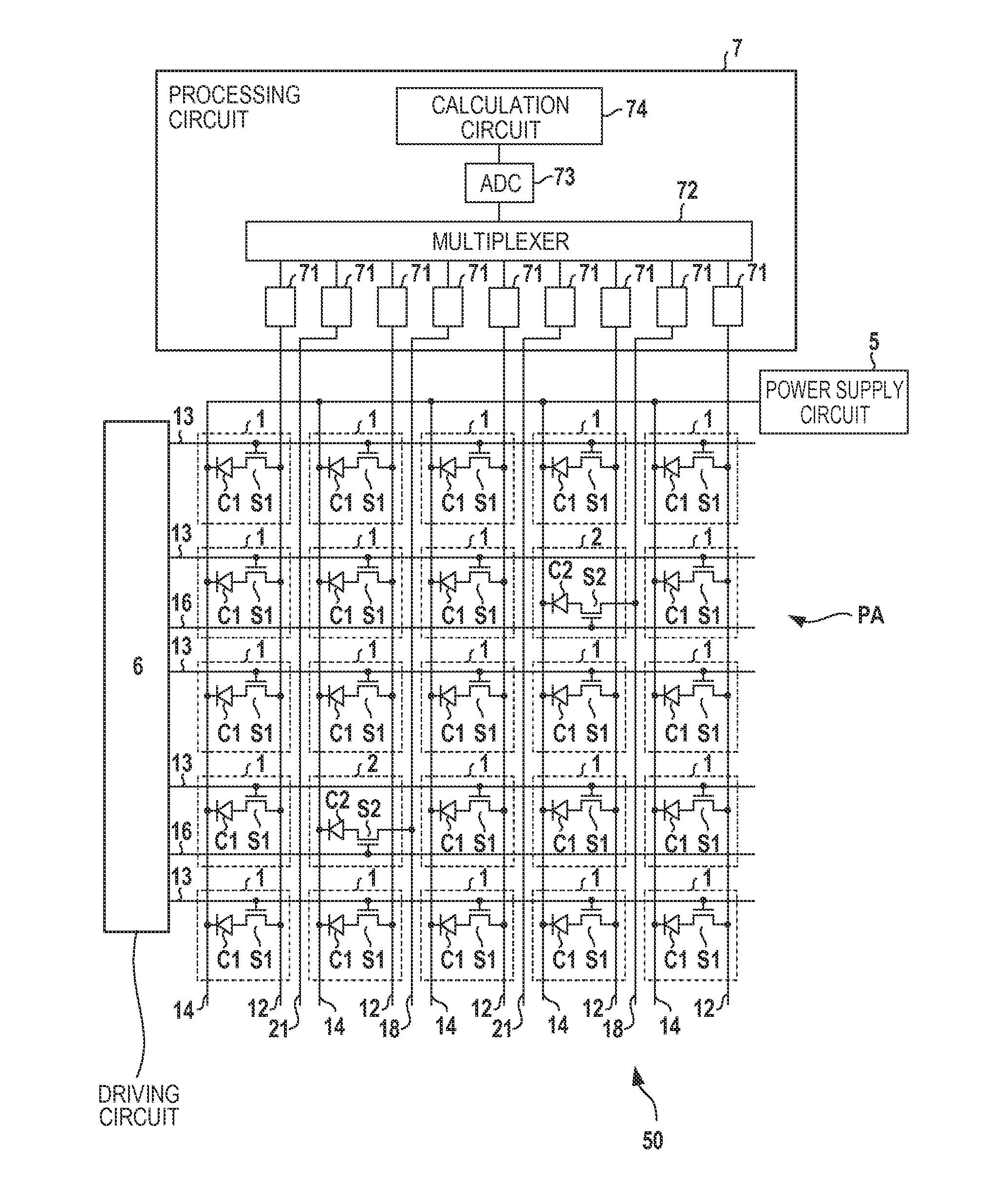
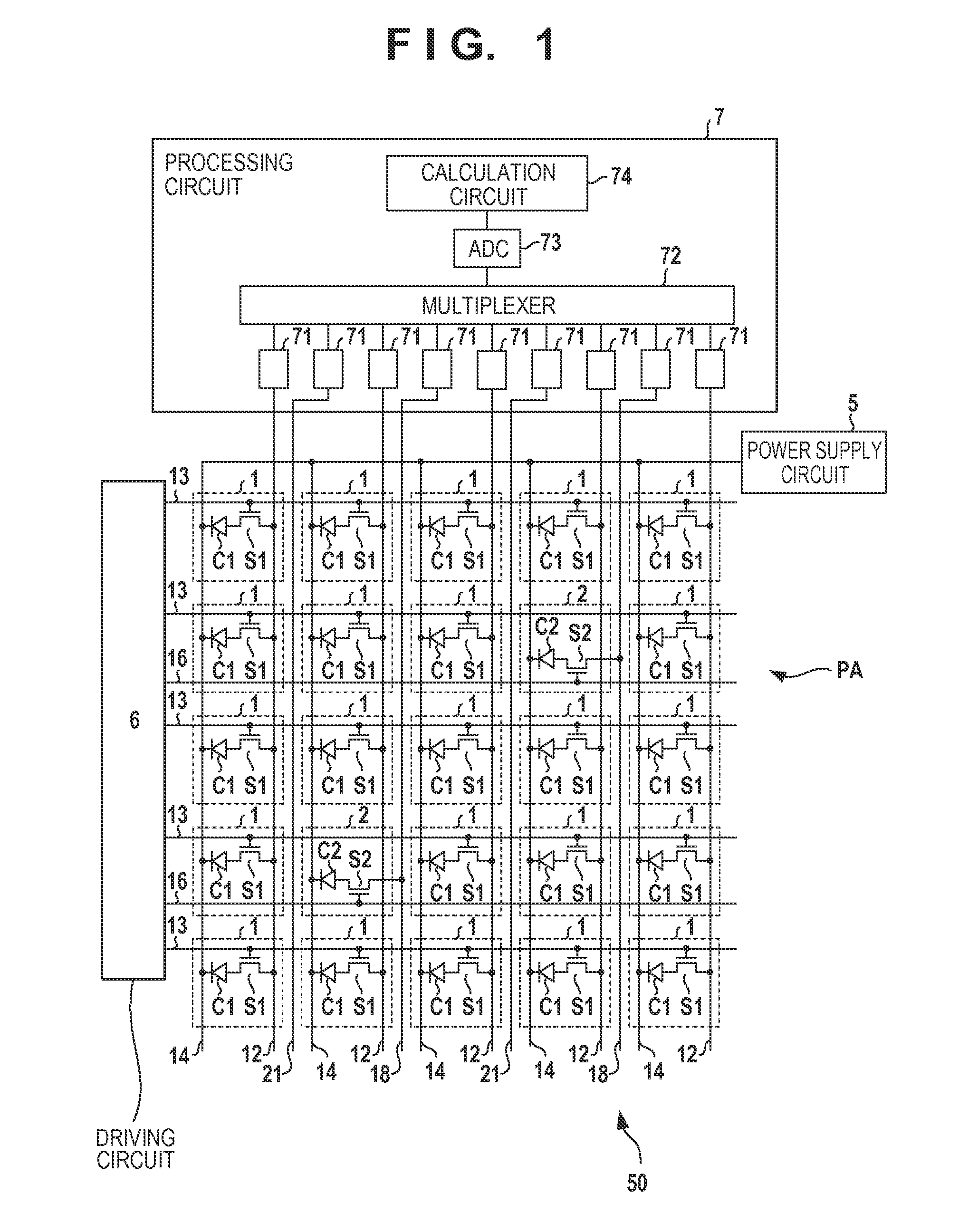
[0038]FIG. 1 is a block diagram showing the arrangement of a radiation imaging apparatus 50 according to the present invention. The radiation imaging apparatus 50 can include a plurality of pixels 1, a plurality of sensors 2, a processing circuit 7, a driving circuit 6, and a power supply circuit 5.
[0039]The plurality of pixels 1 converts radiation into electric signals to obtain a radiation image. The plurality of pixels 1 is arrayed to form an array PA having a plurality of rows and a plurality of columns. Each pixel 1 can include a conversion element C1 which converts radiation into an electric signal and a switch S1 which connects the output electrode of the conversion element C1 to a column signal line 12. The switch S1 can be formed from a TFT (Thin-Film Transistor). A gate line 13 which is driven by the driving circuit 6 is connected to the control electrode (gate electrode) of the switch S1. In this case, one gate line 13 is commonly connected to the pixels on one row. Note ...
third embodiment
[0057]In the third embodiment, a conversion element C1 of the pixel 1 arranged at the position where the sensor 2 (C2, S2) is arranged can be smaller in area than the conversion element C1 of the pixel 1 arranged at another position. However, a difference in sensitivity due to such a difference in area can be corrected by a method similar to shading correction, for example, gain correction and / or offset correction.
[0058]FIG. 7 shows the arrangement of a radiation imaging apparatus 50 according to the fourth embodiment of the present invention. Details which are not mentioned in the fourth embodiment can comply with the first to third embodiments. In the fourth embodiment, each sensor 2 is connected to a column signal line 12. In addition, each second signal line 21 can be arranged to be paired with each column signal line 12 to which the sensor 2 is connected. In the fourth embodiment, the column signal lines 12 function as the first signal lines for transmitting the signals generat...
seventh embodiment
[0063]In addition, in each of regions A to I, the number (first count) of sensors 2 connected to the one column signal line (first signal line) 12 differs from the number (second count) of sensors 2 connected to the other column signal line (second signal line) 12. Each sensor 2 connected to the one column signal line (first signal line) 12 differs from each sensor 2 connected to the other column signal line (second signal line) 12. The processing circuit 7 monitors radiation based on the difference between the value of a signal appearing on the first signal line and the value of a signal appearing on the second signal line. The processing circuit 7 may detect the start and / or end of radiation irradiation based on the sum of a signal appearing on the first signal line and a signal appearing on the second signal line.
[0064]FIG. 12 shows the arrangement of a radiation imaging apparatus 50 according to the eighth embodiment of the present invention. Details which are not mentioned in ...
PUM
 Abstract
Description
Claims
Application Information