Fabrication of nano-sheet transistors with different threshold voltages

a technology of nano-sheet transistors and threshold voltages, applied in the direction of transistors, electrical devices, semiconductor devices, etc., can solve the problems of difficult electrical contact and difficulty in forming individual components

Active Publication Date: 2017-05-16
TESSERA LLC
View PDF5 Cites 121 Cited by
  • Summary
  • Abstract
  • Description
  • Claims
  • Application Information

AI Technical Summary

Benefits of technology

[0007]In accordance with an embodiment of the present invention, a method of forming two or more nano-sheet devices with varying electrical gate lengths is provided. The method includes forming at least two cut-stacks including a plurality of sacrificial release layers and at least one alternating nano-sheet channel layer on a substrate. The method further includes removing a portion of the ...

Problems solved by technology

With ever decreasing device dimensions, forming the indiv...

Method used


Image

  • Fabrication of nano-sheet transistors with different threshold voltages
  • Fabrication of nano-sheet transistors with different threshold voltages
  • Fabrication of nano-sheet transistors with different threshold voltages

Examples


Embodiment Construction

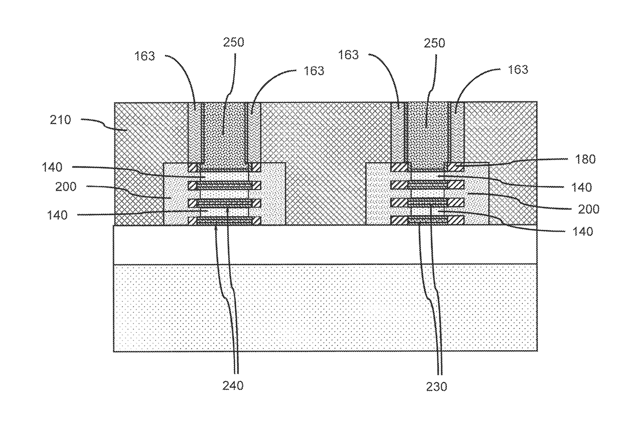
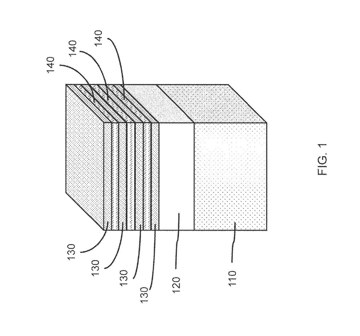
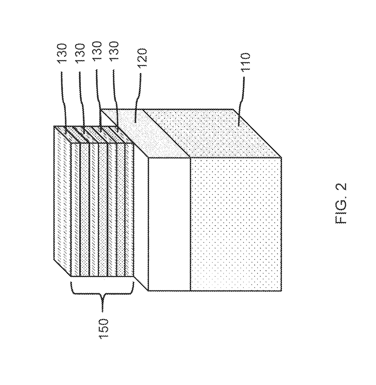
[0031]Principles and embodiments of the present invention relate to fabricating a plurality of transistor devices utilizing nano-sheets for the channel of the devices, where the nano-sheets have different lengths. The electrical gate length, LGe, of the different devices can be varied by using a sequence of etching steps to modify the nano-sheet lengths. The different gate lengths can provide different threshold voltages, VT.

[0032]Principles and embodiments of the present invention also relate to forming nano-sheet transistor devices having different threshold voltages adjacent to each other on the same substrate by controlling the number of etching steps each transistor device undergoes during fabrication. Multiple timed etches can be used to remove predetermined amounts of each exposed nano-sheet channel layer to produce a cut-stack with a predetermined electrical gate length and threshold voltage, while neighboring nano-sheet transistor devices are masked during the etching steps...


PUM


Abstract

A method of forming two or more nano-sheet devices with varying electrical gate lengths, including, forming at least two cut-stacks including a plurality of sacrificial release layers and at least one alternating nano-sheet channel layer on a substrate, removing a portion of the plurality of sacrificial release layers to form indentations having an indentation depth in the plurality of sacrificial release layers, and removing a portion of the at least one alternating nano-sheet channel layer to form a recess having a recess depth in the at least one alternating nano-sheet channel layers, where the recess depth is greater than the indentation depth.

Description

BACKGROUND[0001]Technical Field[0002]The present invention generally relates to the fabrication of two or more nano-sheet transistors on the same substrate having different threshold voltages, and more particularly to forming different sized recesses to provide nano-sheet channels having different gate lengths.[0003]Description of the Related Art[0004]A Field Effect Transistor (FET) typically has a source, a channel, and a drain, where current flows from the source to the drain, and a gate that controls the flow of current through the channel. Field Effect Transistors (FETs) can have a variety of different structures, for example, FETs have been fabricated with the source, channel, and drain formed in the substrate material itself, where the current flows horizontally (i.e., in the plane of the substrate), and finFETs have been formed with the channel extending outward from the substrate, but where the current also flows horizontally from a source to a drain. The channel for the fin...

Claims


Application Information

Patent Timeline
IPC IPC(8): H01L21/336H01L21/311H01L29/66H01L29/06H01L27/088H01L21/02H01L21/338H01L21/00H01L21/8234H01L21/308H01L21/84H01L21/8238
CPCH01L27/088H01L29/0665H01L29/66545H01L21/31111H01L21/02603H01L21/3086H01L21/823431H01L21/823821H01L21/823807H01L21/845H01L21/823412H01L21/84H01L29/0673H01L29/401H01L29/42392H01L29/66439H01L29/775H01L29/78696H01L29/42376H01L29/4983H01L29/78651
Inventor BALAKRISHNAN, KARTHIKCHENG, KANGGUOHASHEMI, POUYAREZNICEK, ALEXANDER
Owner TESSERA LLC
Why Eureka
Try Eureka