Pixel circuit, light-emitting device, and image forming apparatus

A technology for pixel circuits and light-emitting devices, which is applied in the fields of pixel circuits, light-emitting devices and image forming devices, and can solve problems such as insufficient driving of drive transistors, low drive capability, and long time required to change gate potentials, etc.

Inactive Publication Date: 2009-01-07
SEIKO EPSON CORP
View PDF3 Cites 0 Cited by
  • Summary
  • Abstract
  • Description
  • Claims
  • Application Information

AI Technical Summary

Problems solved by technology

[0006] However, if the drive capability of the front-end drive circuit that supplies current to the gate of the drive transistor is low, the drive transistor cannot be sufficiently driven.
If the driving capability is insufficient, it takes a long time to change the gate potential
Therefore, the writing cannot be completed within the predetermined time, resulting in a decrease in printing quality.

Method used


Image

  • Pixel circuit, light-emitting device, and image forming apparatus
  • Pixel circuit, light-emitting device, and image forming apparatus
  • Pixel circuit, light-emitting device, and image forming apparatus

Examples


example 2

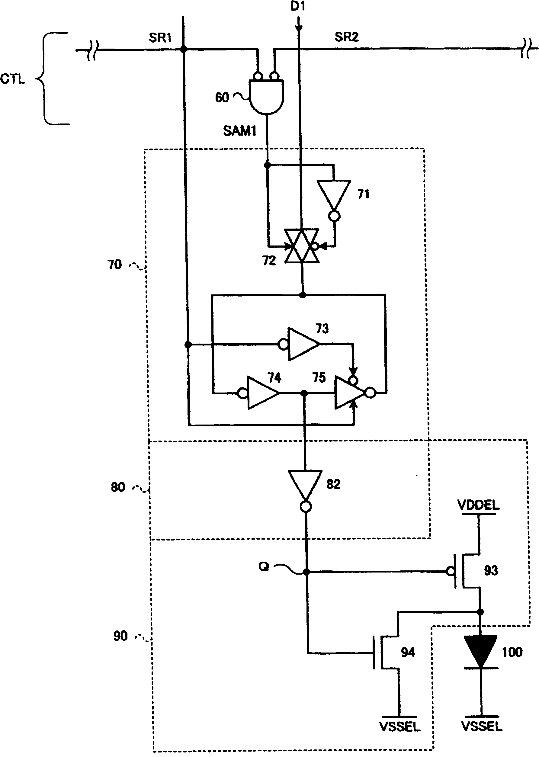
[0062] In the modification column 1 described above, the pixel circuit P is provided with the latch circuit 70 , but instead of the latch circuit 70 , a configuration in which a storage means is formed by a capacitive element may be used.

[0063] Figure 9 It is a circuit diagram showing the configuration of a pixel circuit P according to a modified example. like Figure 9 As shown, the pixel circuit P includes a capacitive element 76 between the gate of the drive transistor 93 and the power supply signal VDDEL on the second high potential side. Therefore, during the active period of the random signal SAM1, the theoretical level of the data signal D1 is written in the capacitive element 76, and the written theoretical level is maintained during the non-active period. Thus, capacitive element 76 functions as storage means 70'.

[0064] Also in this case, since the gate of the drive transistor 93 is controlled by the inverter 82 functioning as the buffer circuit 80, the on / o...


PUM


Abstract

The invention can prevent a pixel circuit from wrongly working. The pixel circuit P of the invention is provided with a control circuit CTL, a latch circuit (70), a cushion circuit (80), a supply circuit (90) and an OLED element (100). The level of the junction Q comes form the output signals of the cushion circuit (80), so that the driving transistor (93) of the supply circuit (90) can be fully driven; thereby increasing the lighting brightness of the OLED element (100) and improving the deviation of the lighting brightness among pixels.

Description

technical field [0001] The present invention relates to a pixel circuit, a light-emitting device and an image forming device using a light-emitting element that emits light of a magnitude corresponding to the amount of current, such as an organic light-emitting diode. Background technique [0002] In recent years, attention has been paid to organic light emitting diodes (Organic Light Emitting Diodes, hereinafter referred to as "OLED elements" as appropriate) as next-generation light-emitting devices that replace liquid crystal elements. An image forming apparatus that utilizes a line head in which a plurality of such OLED elements are arranged in one row as an exposure mechanism is under development. In such a line head, in addition to OLED elements, a plurality of pixel circuits including transistors for driving these are arranged. For example, Patent Document 1 discloses a row head composed of one row of OLED elements. [0003] Here, a plurality of pixel circuits are ar...

Claims


Application Information

Patent Timeline
Patent Type & Authority Patents(China)
IPC IPC(8): G09G3/32H05B33/08H05B44/00
CPCG09G2300/0852G09G2300/0814B41J2/45G09G2300/0857G09G3/3258G09G3/30
Inventor 神田荣二
Owner SEIKO EPSON CORP
Why Eureka
Try Eureka