

Making method of pliable active component array base board
A technology of active components and manufacturing methods, which is applied in semiconductor/solid-state device manufacturing, electrical components, circuits, etc. It can solve the problem that the flexible substrate is not easy to remove, so as to improve the process qualification rate and component characteristics, and avoid the accumulation of charges Effect
- Summary
- Abstract
- Description
- Claims
- Application Information
AI Technical Summary
Problems solved by technology
Method used
Image

Examples
no. 1 example
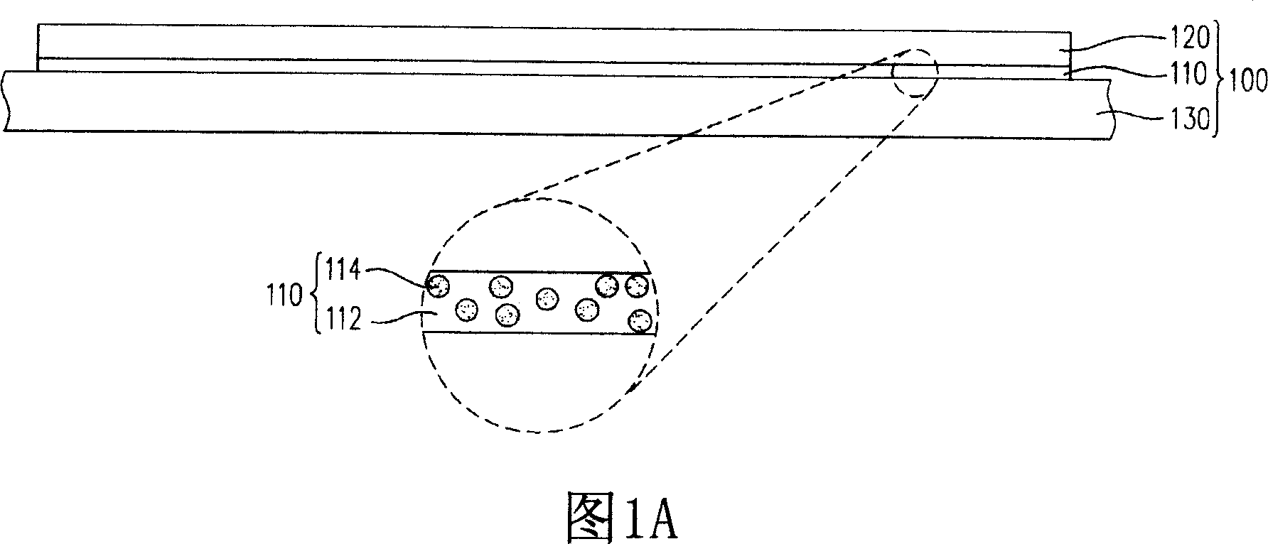
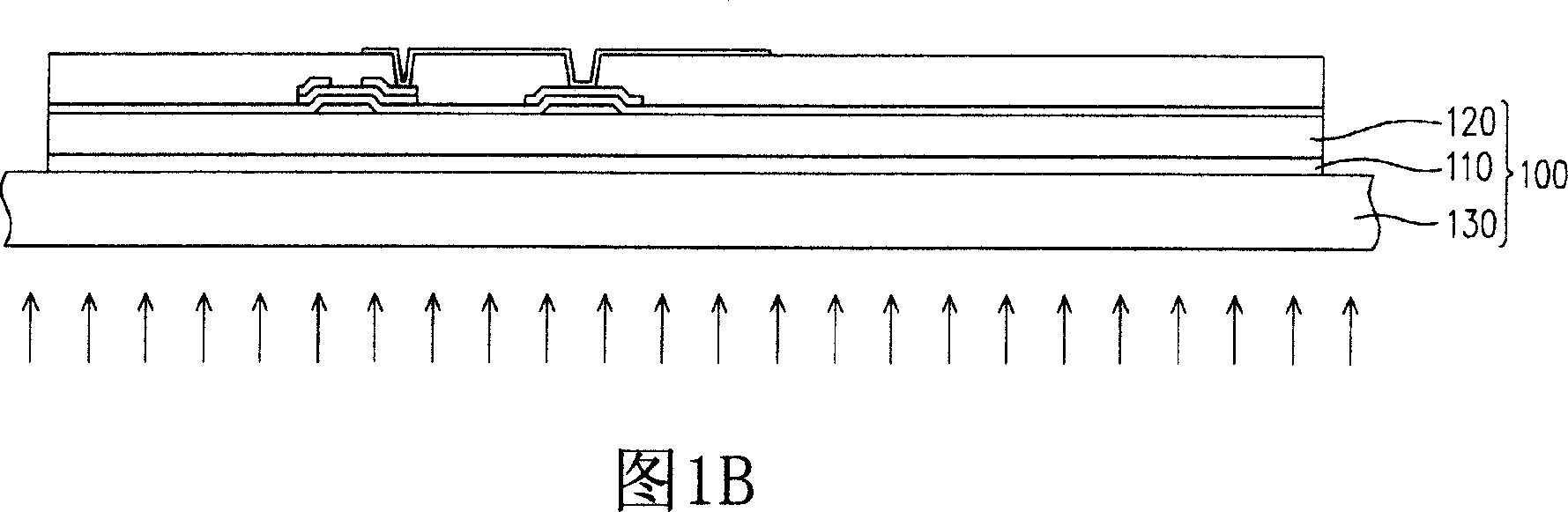
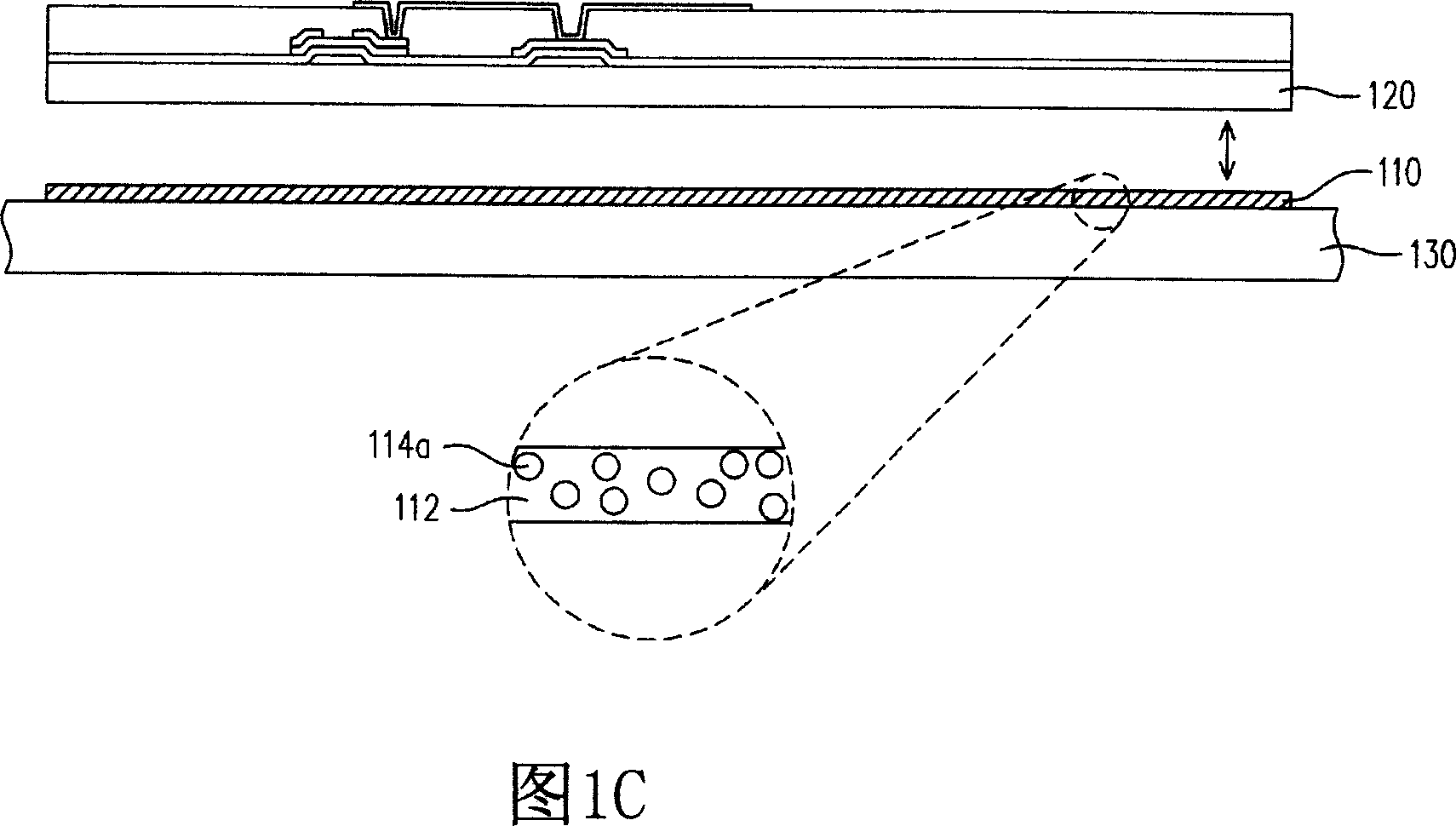
[0038] 1A to 1C are the manufacturing process of the flexible active device array substrate according to the first embodiment of the present invention. First, please refer to FIG. 1A , the flexible substrate 120 is adhered to the rigid substrate 130 by using the adhesive layer 110 to form a substrate module 100 . Wherein, the adhesive layer 110 includes a colloid 112 and sacrificial particles 114 doped in the colloid 112 . In this embodiment, the sacrificial particles 114 include oxide particles, amorphous silicon particles or a combination thereof, and the size of the sacrificial particles 114 is, for example, 0.01 μm to 10 μm. In addition, the flexible substrate 120 is, for example, a plastic substrate, and the rigid substrate 130 is, for example, a glass substrate.
[0039] Next, referring to FIG. 1B , an active device array process is performed on the flexible substrate 120 adhered to the rigid substrate 130 . Wherein, the active element array process includes an amorpho...
no. 2 example
[0043]2A to 2C illustrate the manufacturing process of the flexible active device array substrate according to the second embodiment of the present invention. The manufacturing process of the flexible active device array substrate of this embodiment is similar to that described in the first embodiment. According to the process shown in FIG. 2A to FIG. 2C, the flexible substrate 220 is first adhered to the rigid substrate 230 by using the adhesive layer 210 to form the substrate module 200, and then the flexible substrate 220 adhered to the rigid substrate 230 Perform active element array process. Then, a light source is used to irradiate the adhesive layer 210 , and then the flexible substrate 220 is separated from the rigid substrate 230 .
[0044] The difference between the two is that in this embodiment, the adhesive layer 210 includes a colloid 212 and a sacrificial pattern layer 214 (as shown in FIG. 2A ). Wherein, the material of the sacrificial pattern layer 214 is, f...
no. 3 example
[0049] 3A to 3C illustrate the manufacturing process of the flexible active device array substrate according to the third embodiment of the present invention. The manufacturing process of the flexible active device array substrate of this embodiment is substantially the same as that described in the first embodiment and the second embodiment. The difference is that in this embodiment, the adhesive layer 310 includes a colloid 312 and conductive particles 314 doped in the colloid 312 (as shown in FIG. 3A ). The conductive particles 314 include oxide particles, amorphous silicon particles, or metal particles. Wherein, the material of the metal particles is, for example, gold, silver, copper, titanium oxide or a combination thereof. In addition, the particle size of the conductive particles 314 is, for example, 0.01 μm to 10 μm.
[0050] In the substrate module 300 , the conductive particles 314 are similar to the sacrificial pattern layer 214 of the second embodiment, and both...
PUM
| Property | Measurement | Unit |
|---|---|---|
| Thickness | aaaaa | aaaaa |
| Particle size | aaaaa | aaaaa |
| Wavelength | aaaaa | aaaaa |
Abstract
Description
Claims
Application Information