Organic el display device, organic transistor and methods for manufacturing such organic el display device and organic transistor

A technology of organic transistors and organic light-emitting layers, applied in transistors, semiconductor/solid-state device manufacturing, electric solid-state devices, etc., can solve the problems of reduced component thickness and high production costs

Inactive Publication Date: 2008-04-02
PIONEER CORP
View PDF1 Cites 13 Cited by
  • Summary
  • Abstract
  • Description
  • Claims
  • Application Information

AI Technical Summary

Problems solved by technology

[0008] However, the production cost of this sealing method using these glasses and housings is high and limits reduction in component thickness

Method used


Image

  • Organic el display device, organic transistor and methods for manufacturing such organic el display device and organic transistor
  • Organic el display device, organic transistor and methods for manufacturing such organic el display device and organic transistor
  • Organic el display device, organic transistor and methods for manufacturing such organic el display device and organic transistor

Examples


Embodiment approach 1

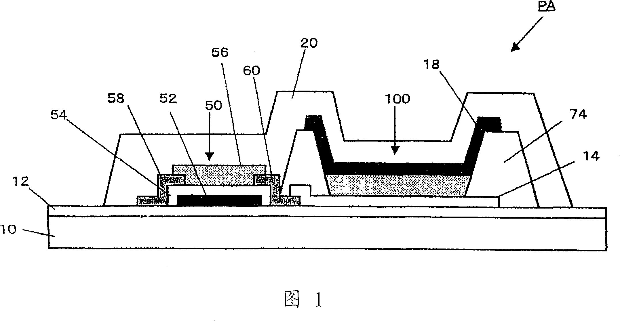
[0130] FIG. 5 shows an organic EL display P2 in Embodiment 1 related to the present embodiment. Since the same reference numerals hereinafter are similar to those in the above-described embodiments, descriptions thereof are omitted.

[0131] The organic EL element 100 having a top emission structure is arranged on the organic TFT 50 , and the organic EL element 100 and the organic TFT 50 are covered with a protective film 20 . The cathode 18 of the organic EL element is formed so as to cover the interlayer insulating film on the organic TFT. The organic semiconductor layer 56 of the organic TFT 50 is made of an n-type organic semiconductor. The drain electrode 60 and the cathode electrode 18 are electrically connected by a via hole 80 which is a charge transfer path in the interlayer insulating film 72 .

[0132] A method of manufacturing the organic EL display P2 will be described. A barrier film 12 is formed on the substrate 10 to produce an organic TFT 50 . An interlaye...

Embodiment approach 2

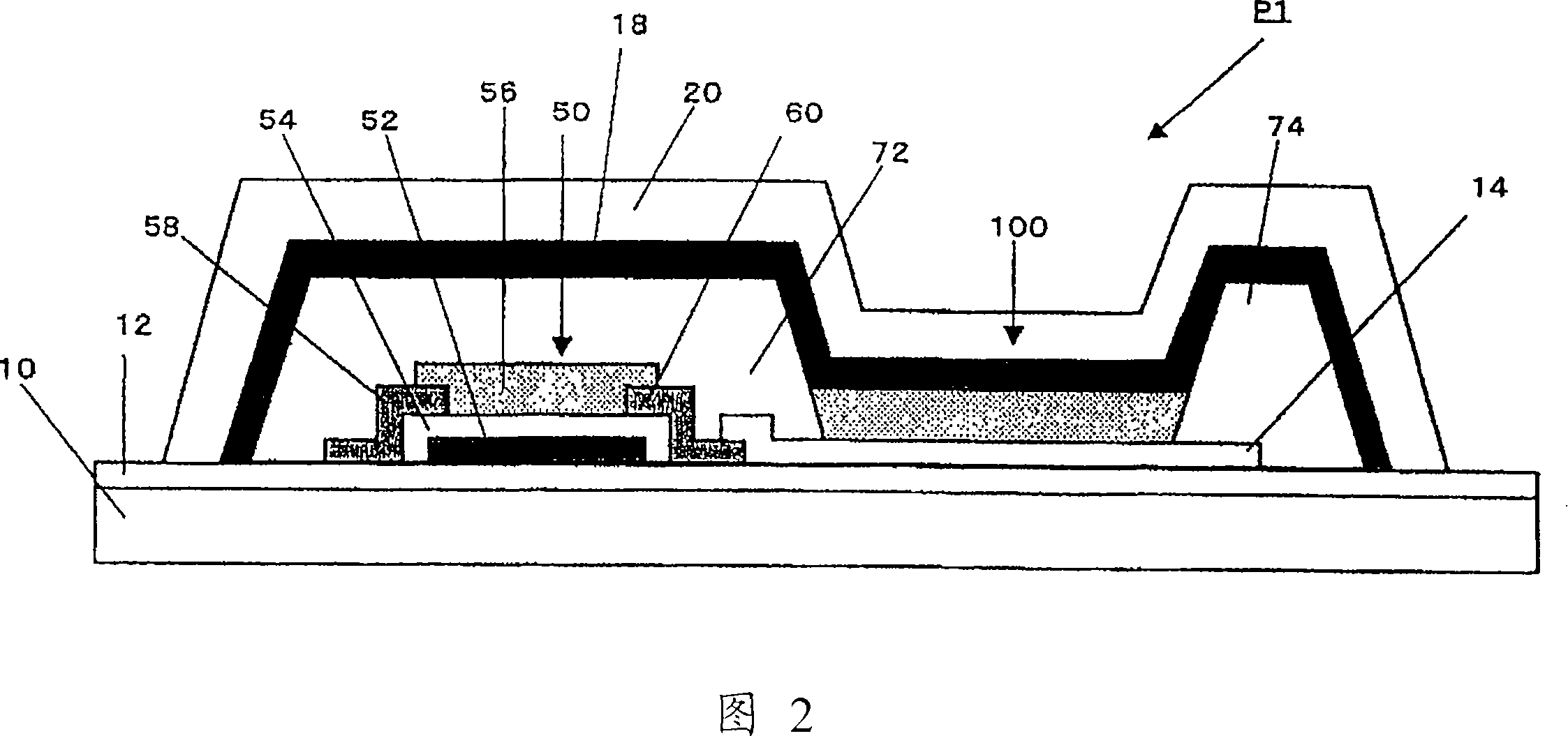
[0136] FIG. 6 shows an organic EL display P3 related to another embodiment 2 of the present embodiment.

[0137] The organic TFT 59 for driving is arranged on the organic TFT 50 for switching, the top contact type organic EL element 100 is arranged on the organic TFT 59, and the organic EL element 100, the organic TFT 50, and the organic TFT 59 are covered with a protective film 20 . In the case where the driving transistor is a static induction transistor (SIT) as shown in FIG. 6 , the drain of the organic TFT 59 is fabricated to entirely cover the organic TFT 50 and the organic TFT 59 . The semiconductor layers of organic TFT 50 and organic TFT 59 are n-type organic semiconductors. The organic TFT 59 is composed of a source 57 / gate 51 / drain (the anode 14 of the organic EL element 100 ).

[0138] The drain 60 and the source 57 of the organic TFT 59 are electrically connected by a via 80 ; the via 80 is an electron-hole transport path in the interlayer insulating film 72 ....


PUM


Abstract

An organic EL display device wherein deterioration of organic transistor performance is reduced, a method for manufacturing such organic EL display device, an organic transistor and a method for manufacturing such organic transistor are provided. The organic EL display device (P1) covers the organic transistor (50), and is provided with a protection film (20) for protecting the organic transistor. The organic EL display device includes a conductive layer (a cathode of an organic EL element (100)) (18) between the protection film (20) and a front plane of the organic transistor (50), and an insulating film (72) formed closer to the front plane side of the organic transistor (50) than the conductive layer (18) for insulating the front plane of the organic transistor (50) from the conductive layer (18).

Description

technical field [0001] The present invention relates to an organic EL display, a method of manufacturing the organic EL display, an organic transistor, and a method of manufacturing the organic transistor. Background technique [0002] Organic transistors are used in a wide variety of applications. For example, it is used as a tool for driving organic EL elements in organic EL displays. [0003] The organic EL element is equipped with an electrode on a substrate and an organic solid layer having at least a light-emitting layer between the electrodes, wherein electrons and electron holes are injected into the light-emitting layer in the organic solid layer from the electrodes on both sides to Light is emitted in the organic light-emitting layer, and high-intensity light emission can be obtained. In addition, it is characterized by a wide selectivity of luminescent colors because the luminescence of organic compounds is used. Therefore, it is expected as a light source and ...

Claims


Application Information

Patent Timeline
Patent Type & Authority Applications(China)
IPC IPC(8): H01L27/32H01L29/786H01L51/05H01L51/50
CPCH01L27/3248H01L27/3246H01L51/0078H01L27/3274H01L51/0059H01L27/3272H01L51/0545H01L51/0081H10K59/122H10K59/123H10K59/125H10K59/126H10K85/631H10K85/311H10K85/324H10K10/466
Inventor 原田千宽中马隆大田悟吉泽淳志
Owner PIONEER CORP
Why Eureka
Try Eureka