

Soldered ball surface defect detection device and method based on machine vision
A technology of machine vision and defect detection, applied in the direction of measuring devices, instruments, scientific instruments, etc., can solve the problems of ineffective detection of solder ball surface defects, affecting chip quality, high false detection rate, etc., and achieve accurate detection of solder ball surface defects , Simple device structure and strong classification ability
- Summary
- Abstract
- Description
- Claims
- Application Information
AI Technical Summary
Problems solved by technology
Method used
Image

Examples
Embodiment Construction
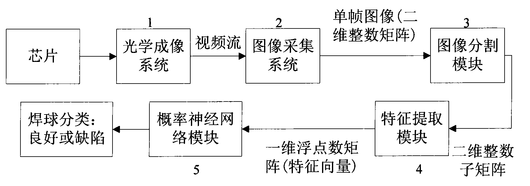
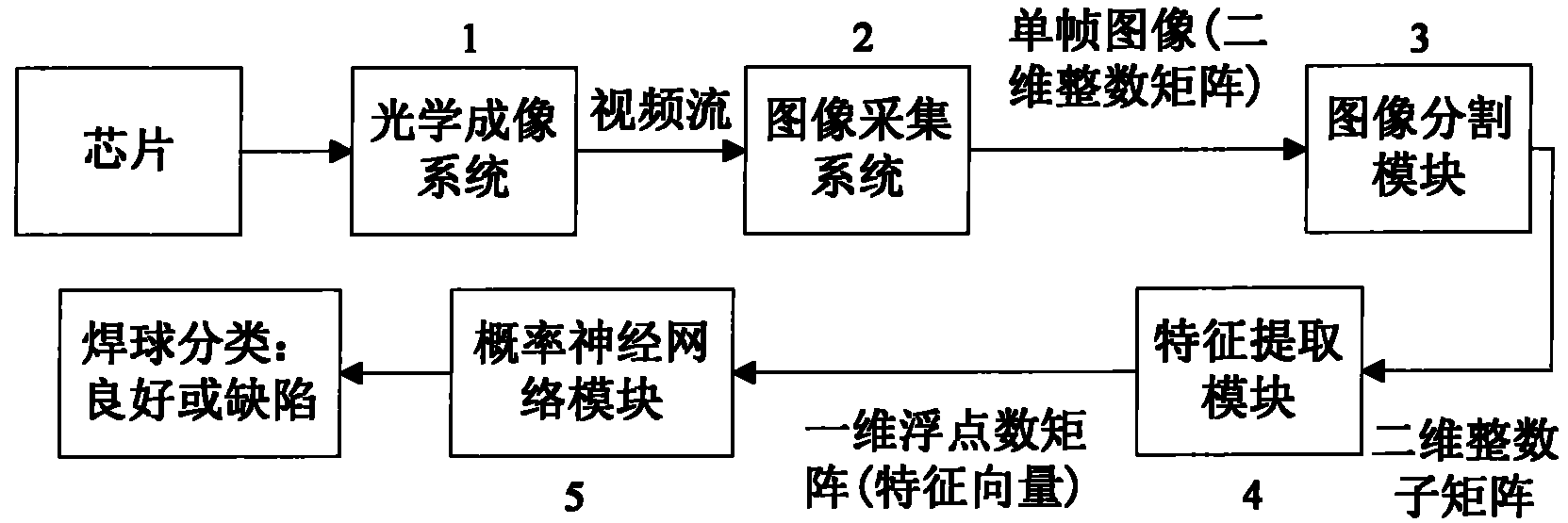
[0035] The embodiments of the present invention are described in detail below in conjunction with the accompanying drawings: this embodiment is implemented on the premise of the technical solution of the present invention, and detailed implementation methods and specific operating procedures are provided, but the protection scope of the present invention is not limited to the following the described embodiment.
[0036] Such as figure 1 As shown, the machine vision-based solder ball surface defect detection device involved in this embodiment is composed of an optical imaging system 1, an image acquisition system 2, an image segmentation module 3, a feature extraction module 4 and a probabilistic neural network module 5, wherein:
[0037] Optical imaging system 1 adopts a black and white CCD camera to collect chip images;
[0038] The image acquisition system 2 receives the chip image from the black-and-white CCD camera and transmits it to the computer, uses software to trigge...
PUM
 Abstract
Description
Claims
Application Information