

Detection method for silicon wafer warpage degree
A detection method and wafer technology, applied in the detection of whether the warpage degree of the wafer will affect the subsequent process, the detection process field, can solve the problem of not being able to detect the uniformity of the wafer warpage, and achieve the effect of eliminating position anomalies
- Summary
- Abstract
- Description
- Claims
- Application Information
AI Technical Summary
Problems solved by technology
Method used
Image

Examples
Embodiment Construction
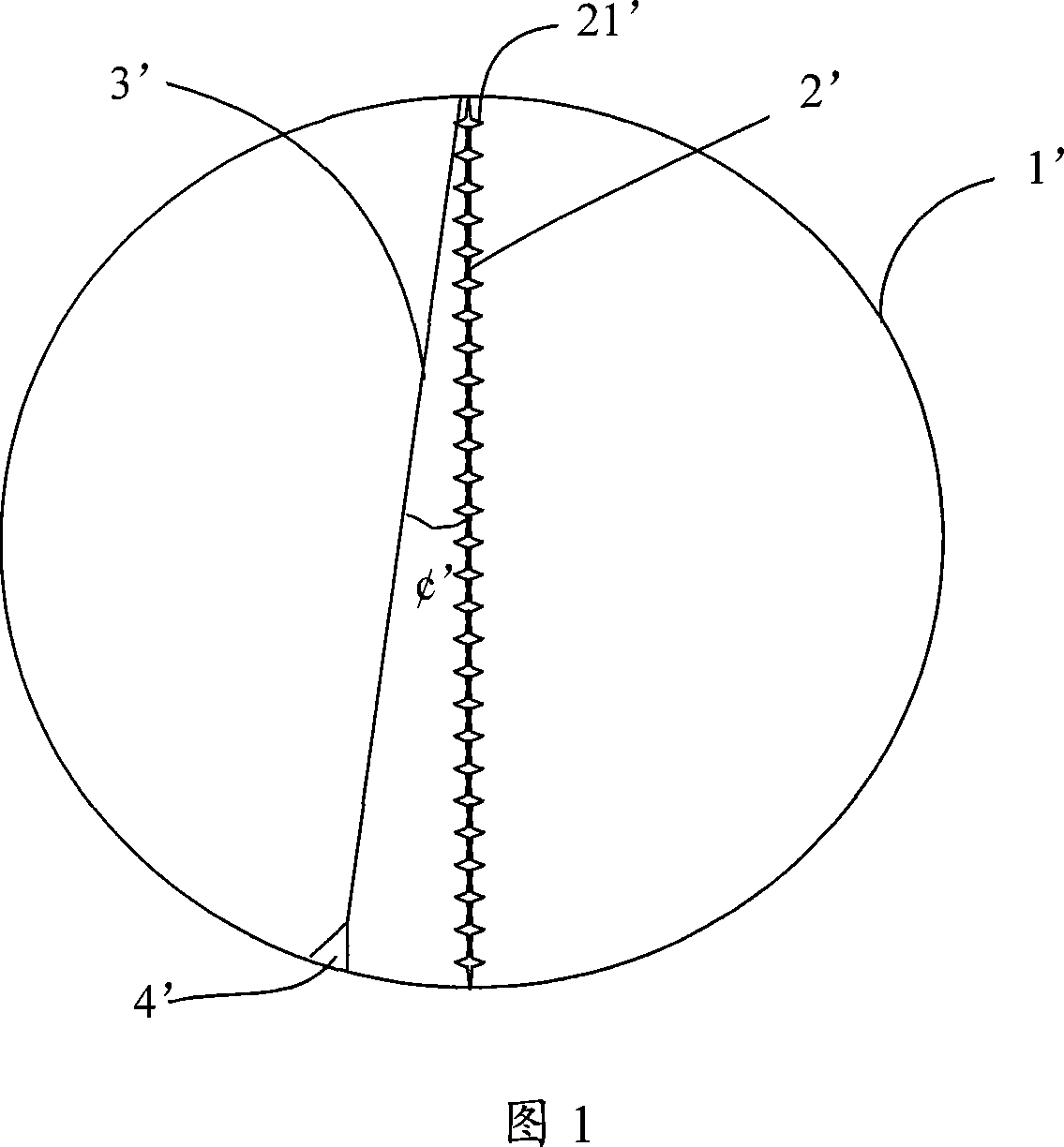
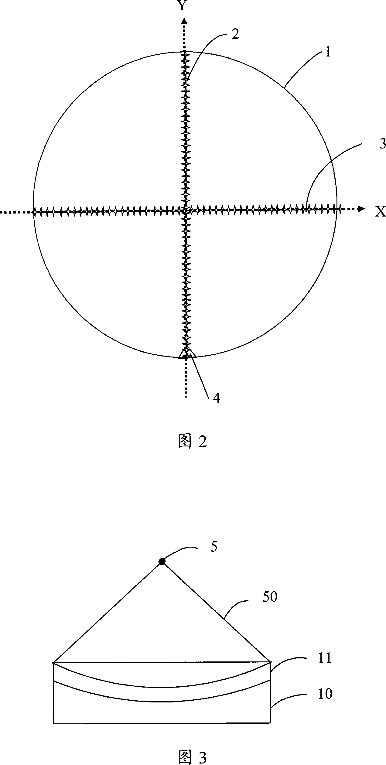
[0011] The preferred embodiments of the method for detecting the degree of wafer warpage provided by the present invention will be described in detail below in conjunction with the accompanying drawings, in order to further understand the technical solution, purpose and beneficial effects of the invention. The present invention can be applied in any process, but in this embodiment, the process of the wafer is a thermal oxidation step for forming an oxide film on the surface of the wafer.
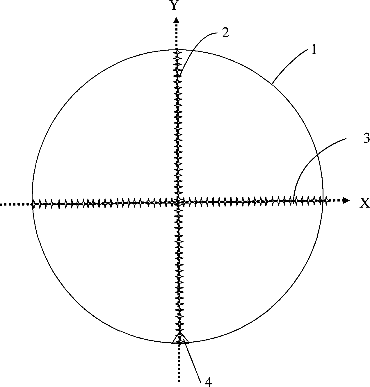
[0012] see figure 2 with image 3 A wafer 1 includes a substrate 10 and an oxide film 11 formed on the substrate in a thermal oxidation step. The detection method of this embodiment is used to detect whether the warpage of the wafer 1 after the thermal oxidation step will affect the subsequent manufacturing process. This detection method comprises the steps:
[0013] The wafer is provided with a mark notch 4, first select two detection lines 2 and 3 crossing the center of the wafer in tw...
PUM
 Abstract
Description
Claims
Application Information