
Regional image display dimension setting method

A technology of display size and screen display, applied in special data processing applications, instruments, electrical digital data processing, etc., to achieve the effect of improving efficiency and reducing work intensity

Inactive Publication Date: 2009-07-08
SHENZHEN SHENGXUNDA TECH
View PDF0 Cites 2 Cited by
  • Summary
  • Abstract
  • Description
  • Claims
  • Application Information

AI Technical Summary

Problems solved by technology

[0004] The current electronic aided design EDA tools (i.e. PCB design tools) only use dragging to zoom in and out for the entire PCB design file, and do not distinguish between different display sizes according to different areas

Method used


Image

  • Regional image display dimension setting method

Examples


Embodiment Construction

[0023] The specific implementation manner of the present invention will be further described in detail below in conjunction with the accompanying drawings and examples, but the protection scope of the present invention should not be limited thereby.

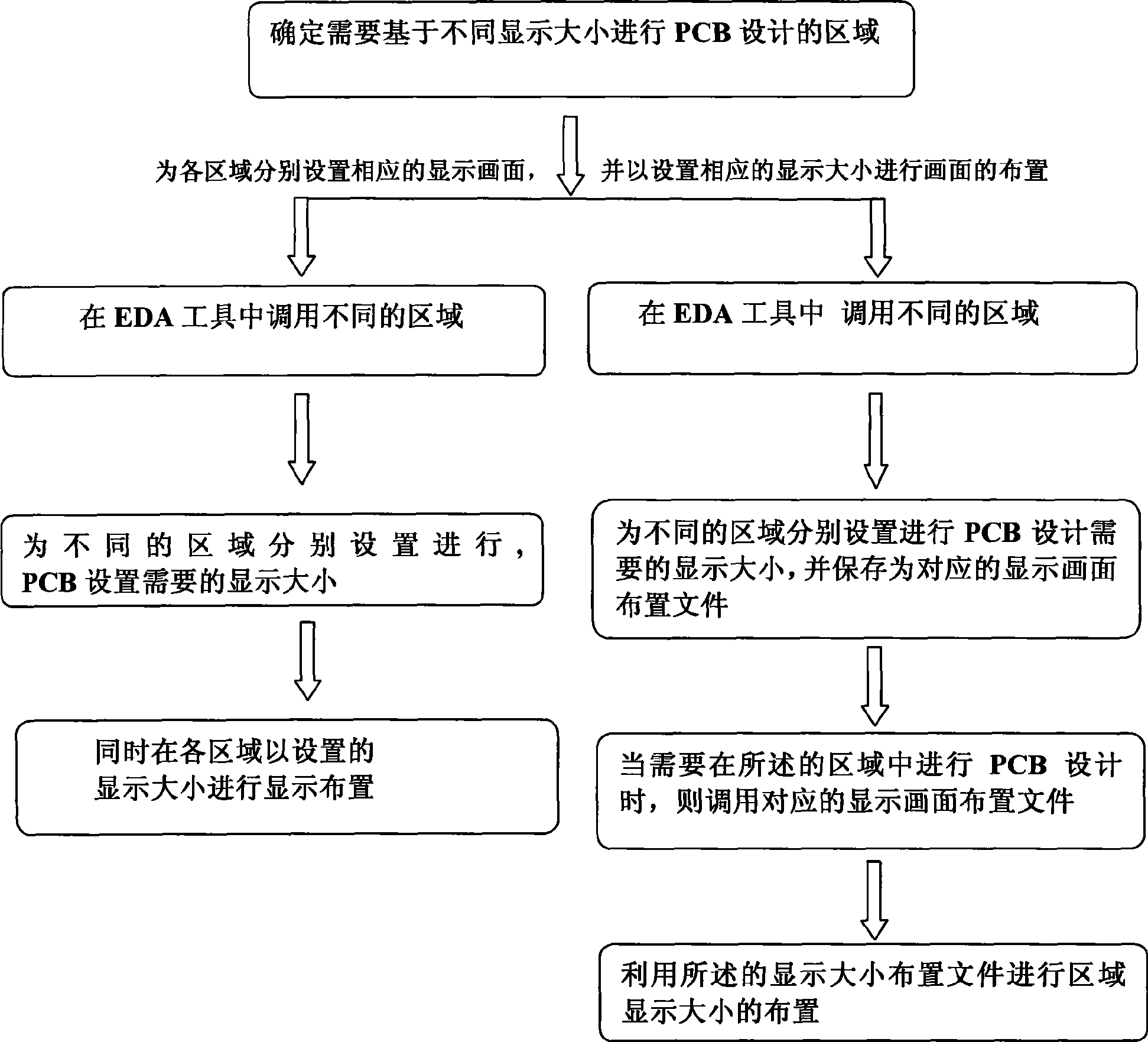
[0024] The core of the present invention is to provide an effective display size method for the PCB design tool, so that different areas can be provided with the display sizes required by the design in the PCB design process, and different areas correspond to different display size arrangements. For example, in the BGA area, a relatively enlarged picture is required when routing due to the high pin density. The devices in the QUAD package can have a smaller screen than the display ratio. In order to meet the display ratio of different areas, the engineer only needs to set the unused display size of multiple areas at one time. In the future design, there is no need to frequently drag to adjust the size of the screen. As long as th...


PUM


Abstract

The invention discloses a method for setting the display size of a regional picture. The method comprises the following steps: step 1, regions required for PCB design on the basis of various display pictures during the process of the PCB design are determined; and step 2, the corresponding display sizes are set for the regions respectively, and the corresponding display pictures are set in each region of a PCB file. The invention provides a manner for realizing the regionalization display management in an EDA tool, that is, various display sizes are set in a partitioning manner, so that no matter how frequent the switching is performed among various regions during the process of the PCB design, the design can be conveniently performed on the basis of various display sizes. The invention avoids the reduction in the PCB design efficiency due to the frequent switching of the display sizes of the pictures during the process of the PCB design, that is, the invention ensures that the PCB design efficiency is greatly improved, and the working strength of a PCB designer is relieved.

Description

technical field [0001] The invention relates to PCB design, in particular to a method for setting the display size of an area picture. Background technique [0002] With the development of electronic technology and the demand of PCB design, various PCB design tools are continuously provided to PCB designers. [0003] During the PCB design process, in order to improve the efficiency of the design, it is usually necessary to provide a corresponding display size in the area where the PCB design is performed. That is to say, in the PCB design process, different areas in the PCB file page require different display sizes according to the actual situation, so that the designer can plan the design in the case of full and partial display, and the design has density. For different devices, when routing the area where these devices are located, it is necessary to display an appropriate size to facilitate routing. [0004] The current electronic aided design EDA tools (i.e. PCB design...

Claims


Application Information

Patent Timeline
Patent Type & Authority Applications(China)
IPC IPC(8): G06F17/50
Inventor 周孝梅刘建华
Owner SHENZHEN SHENGXUNDA TECH
Learn More