Method for realizing regional grid points in PCB design
An implementation method and grid point technology, applied in the electronic field, can solve the problems of cumbersome grid system implementation, low PCB design accuracy and design efficiency, and grid point not being widely used, so as to reduce work intensity, improve efficiency, The effect of improving quality
- Summary
- Abstract
- Description
- Claims
- Application Information
AI Technical Summary
Problems solved by technology
Method used
Image

Examples
Embodiment Construction
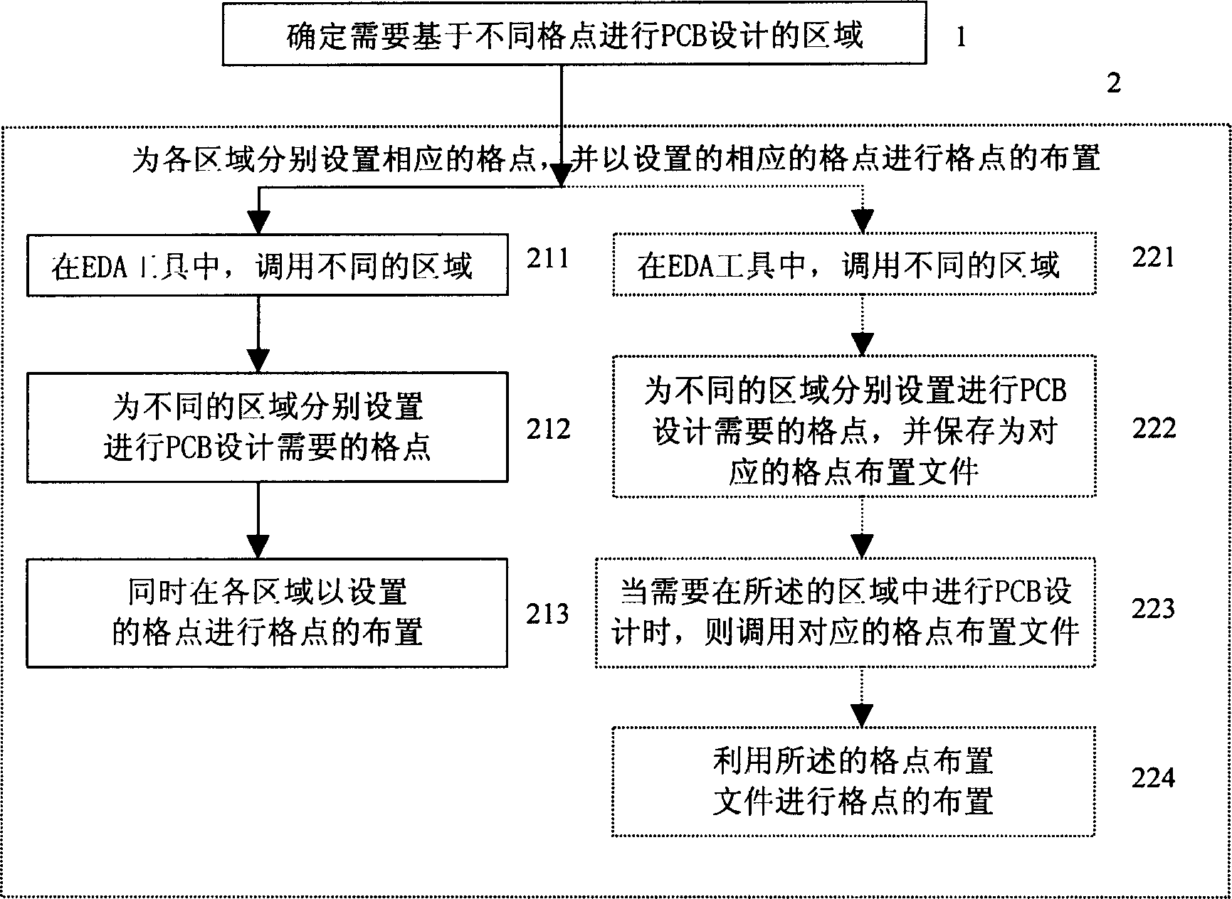
[0034] The core of the present invention is to provide an effective grid point layout method for PCB design tools, so that different areas can be provided with grid points required for design during the PCB design process, and different areas correspond to different grid point layout methods. For example, a 1MM BGA provides 0.5MM grid points, and a 1.27MM BGA provides 25mil grid points, etc.; in this way, CAD engineers only need to complete the grid point setting once, and there is no need for frequent grid point setting in future designs. set up.
[0035] In a nutshell, the present invention sets different grid points for different areas, and can be divided into two situations in the process of grid point arrangement for each area: one is to use different grid points corresponding to different areas At the same time, it is arranged in the PCB design file. When the PCB designer switches and designs in different areas, there is no need to perform grid layout operations; the oth...
PUM
 Abstract
Description
Claims
Application Information