Multichip package structure capable of arranging chips on pins

A multi-chip packaging and chip technology, applied in electrical components, electrical solid devices, circuits, etc., can solve the problems of shortening the stackable height of chips, limiting the number of stackable chips, and inability to stack chips, etc., so as to reduce the risk of wire punching and reduce The effect of mold flow interference and avoiding wrong line

Inactive Publication Date: 2011-01-26
POWERTECH TECHNOLOGY
View PDF0 Cites 0 Cited by
  • Summary
  • Abstract
  • Description
  • Claims
  • Application Information

AI Technical Summary

Problems solved by technology

In addition, in order to prevent the second chip 140 from mistakenly touching the first bonding wires 160 located below, a spacer 190 is usually provided between the first chip 130 and the second chip 140, but this also shortens the possible time of the chip. stack height without being able to stack more chips
Because the peripheral portion of the second chip 140 that is not bonded to the spacer 190 (including the portion where these second solder pads 143 are formed) cannot obtain support from the spacer 190 and become a floating position when bonding, in order To make these second bonding wires 170 have better wire bonding support, the second chip 140 must have a certain thickness, but this also limits the number of chips that can be stacked.

Method used


Image

  • Multichip package structure capable of arranging chips on pins
  • Multichip package structure capable of arranging chips on pins
  • Multichip package structure capable of arranging chips on pins

Examples


no. 1 Embodiment

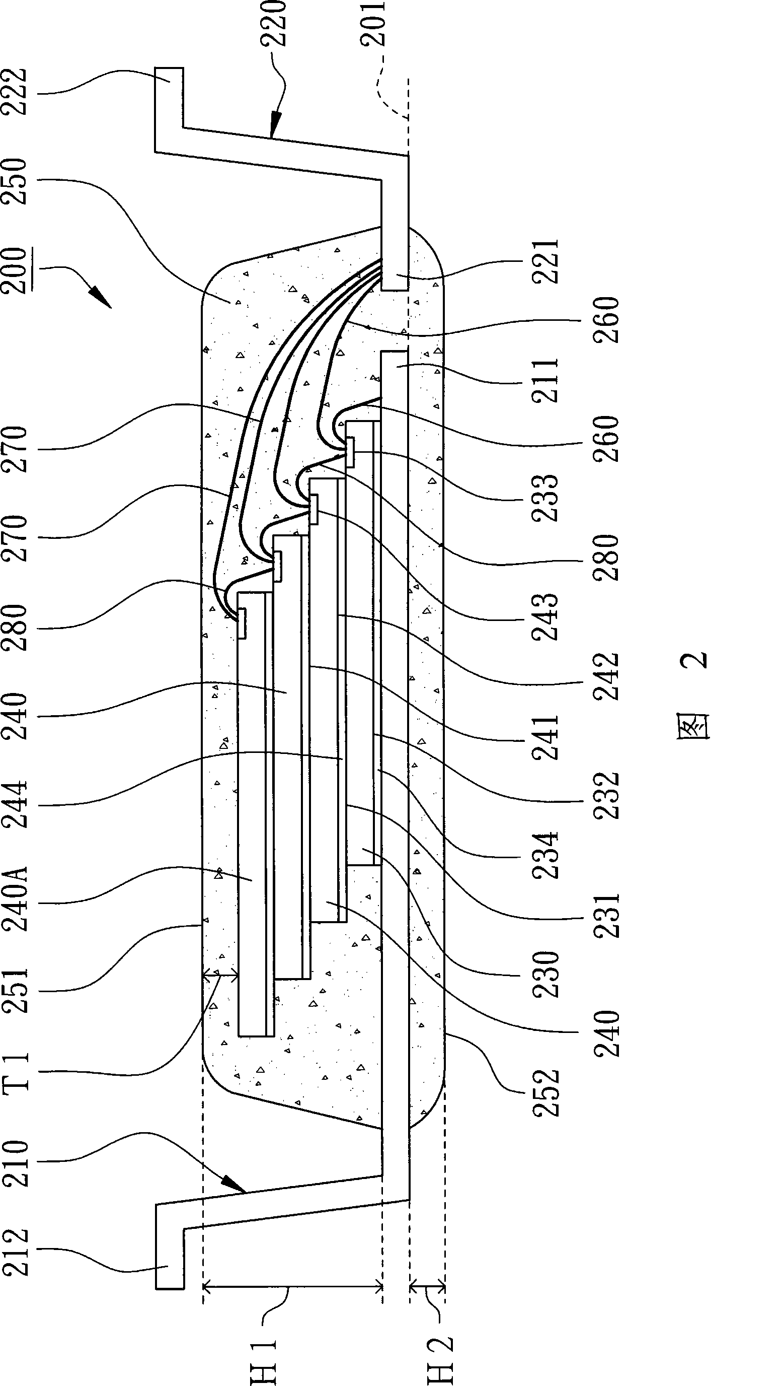
[0059] According to the first specific embodiment of the present invention, as shown in FIG. 2 , a chip-on-pin multi-chip package structure 200 mainly includes two or more first pins 210, a first chip 230, one or more More second chips 240 and encapsulant 250 .

[0060] Please refer to FIG. 2, each first pin 210 has a first inner leg 211 and a first outer leg 212, wherein the "inner leg" is the part where the pin is sealed in the sealing body 250; " The “outer leg portion” refers to the portion where the lead extends outside the encapsulant 250 . These first pins 210 can belong to the same lead frame, which can be made of iron, copper or other metal materials, and have an appropriate thickness (about 0.125 mm or more), enough to carry the first chip 230 and the second chip. 240 structural strength. Preferably, the thickness of the first pins 210 may not be smaller than the thickness of the first chip 230 . Moreover, the first inner legs 211 are coplanar and fully submerged....

no. 2 Embodiment

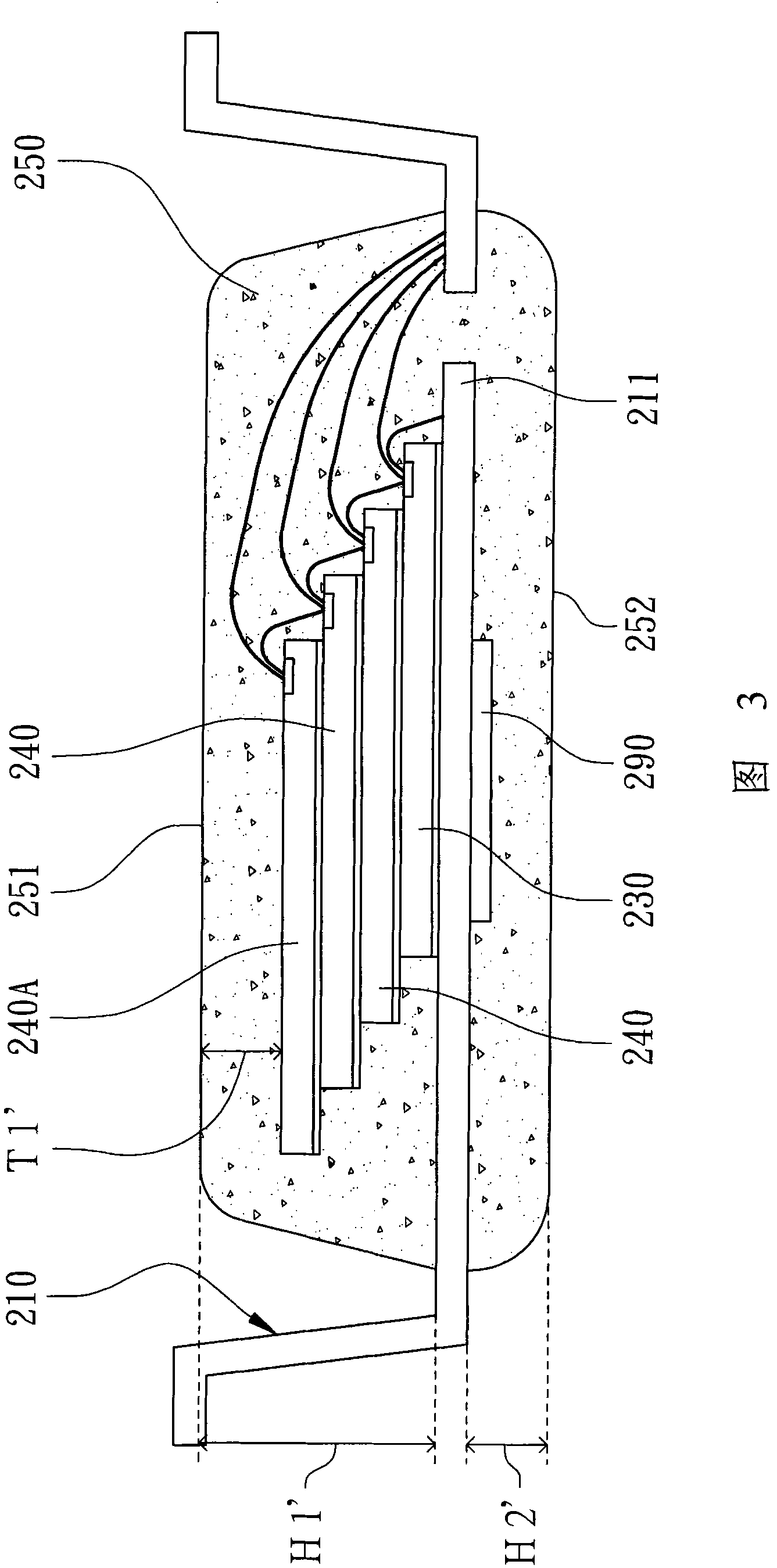
[0070] In the second specific embodiment of the present invention, please refer to FIG. 3 , which discloses another multi-chip package structure with chips on pins. Its main structure is roughly the same as that of the first specific embodiment of the present invention, so the The symbols of the first specific embodiment will not be repeated. The multi-chip package structure mainly includes two or more first pins 210 , a first chip 230 , one or more second chips 240 and an encapsulant 250 . In this embodiment, the height distance H1' from the first inner legs 211 of the first pins 210 to the first surface 251 of the molding body 250 is approximately The height distance H2' of the two surfaces 252 is three times, and the number of the second chips 240 is appropriate, so that the height distance H2' from the first inner legs 211 to the second surface 252 of the encapsulant 250 is approximately the same The thickness T1 ′ of the encapsulant 250 from the first surface 251 to the ...


PUM


Abstract

The invention discloses a multichip package structure capable of arranging chips on pins. The multichip package structure mainly comprises two or more two pins, a first chip arranged on the pins, a second chip or more second chips overlaid on the first chip and an adhesive body; the inner parts of the pins, which are in the adhesive body, are completely sunken on the same plane so that the inner parts of the pins are completely parallel to the upper surface and the lower surface of the adhesive body; the height distance between the inner parts of the pins and the upper surface of the adhesivebody is three times or more of the height distance between the inner parts of the pins and the lower surface of the adhesive body; and the quantity of the second chip(s) is proper so that the thickness between the upper surface of the adhesive body and the nearest second chip is approximately identical to the height distance between the inner parts of the pins and the lower surface of the adhesivebody. The balance of upper mold flow and lower mold flow can be achieved although the inner parts of the pins are not bent for sinking, therefore the pins supporting the multiple chips cannot displace or incline.

Description

technical field [0001] The present invention relates to a semiconductor device, in particular to a chip-on-lead (COL, Chip-On-Lead) multi-chip packaging structure. Background technique [0002] In the traditional semiconductor packaging structure, the lead frame can be used as a chip carrier and an electrical transfer medium. Depending on the way the chip is carried, the packaging form can be divided into: chip on the lead (COL, Chip-On-Lead), lead The pin is on the chip (LOC, Lead-On-Chip) and the chip is carried on the chip pad (die pad) of the lead frame. Wherein, "the chip is on the lead" refers to adhering the back of the chip (ie, the surface without integrated circuits) to the inner section of the lead, and then sealing the chip and the lead with an encapsulant. In order to achieve a balance between the upper and lower mold flow during the injection molding process, the tie bar of the lead or chip pad is usually made into multiple sinking bends, which will cause the ...

Claims


Application Information

Patent Timeline
Patent Type & Authority Patents(China)
IPC IPC(8): H01L25/00H01L25/065H01L23/488H01L23/31
CPCH01L2224/48247H01L2224/48145H01L2224/32245H01L2224/73265H01L2224/32145H01L2225/06562H01L24/73H01L2924/14H01L2924/181
Inventor 范文正
Owner POWERTECH TECHNOLOGY
Why Eureka
Try Eureka