Supercharge Your Innovation With Domain-Expert AI Agents!

Liquid crystal display panel

A liquid crystal display panel and display area technology, applied in nonlinear optics, instruments, optics, etc., can solve the problems affecting the characteristics of liquid crystal display panel 1, uneven gaps, uneven colors, etc., to ensure characteristics and display quality, and improve products. The effect of improving yield and process yield

Active Publication Date: 2012-12-19
INNOLUX CORP
View PDF3 Cites 0 Cited by
  • Summary
  • Abstract
  • Description
  • Claims
  • Application Information

AI Technical Summary

Problems solved by technology

[0004] Please refer to Figure 1B As shown, when the liquid crystal display panel 1 is used in an upright manner for a long time, or when the viscosity coefficient of the liquid crystal is reduced due to operation in a high temperature environment, the effect of gravity will make the liquid crystal layer 13 flow toward the bottom of the liquid crystal display panel 1, resulting in The gap (gap) between the color filter substrate 11 and the thin film transistor substrate 12 at the bottom position of the liquid crystal display panel 1 is not uniform, which affects the characteristics of the liquid crystal display panel 1, thus causing abnormal color unevenness and reducing its display quality. A phenomenon known as gravity MURA (color unevenness)
[0005] In addition, if contamination or small air bubbles are generated around the sealant 14 of the liquid crystal display panel 1 during the manufacturing process, these pollution or small air bubbles may also flow into the display area along with the liquid crystal layer 13, affecting the reliability and use of the liquid crystal display panel 1. life

Method used


Image

  • Liquid crystal display panel
  • Liquid crystal display panel
  • Liquid crystal display panel

Examples


Embodiment Construction

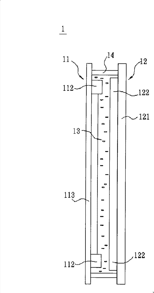
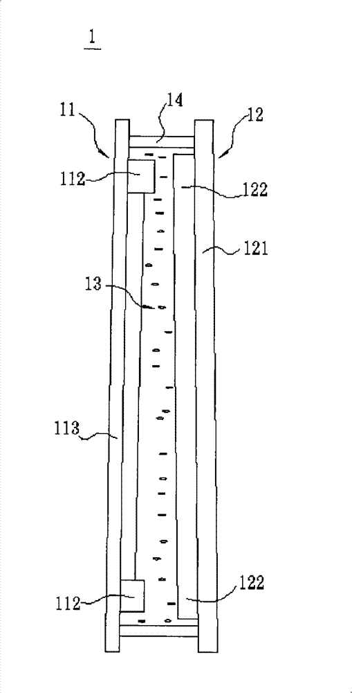
[0038] A liquid crystal display panel according to a preferred embodiment of the present invention will be described below with reference to related drawings, wherein the same elements will be described with the same reference symbols.

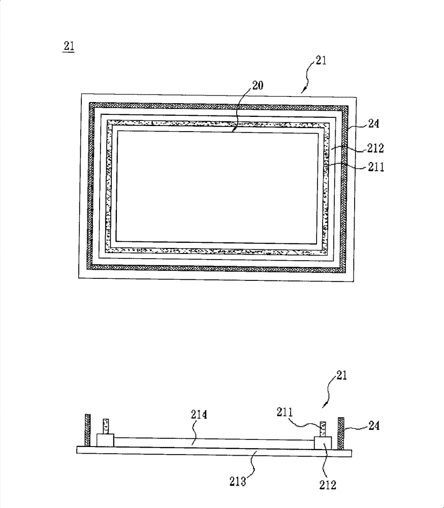
[0039] Please refer to Figure 2A to Figure 2C As shown, a liquid crystal display panel 2 according to a preferred embodiment of the present invention includes a color filter substrate 21 and a thin film transistor substrate 22 . A liquid crystal layer 23 is sandwiched between the color filter substrate 21 and the thin film transistor substrate 22, the liquid crystal display panel 2 has a display area 20, and a frame glue 24 is arranged between the color filter substrate 21 and the thin film transistor substrate 22, the frame glue 24 Located outside the display area 20. The color filter substrate 21 and the TFT substrate 22 respectively have a first tenon structure 211 and a second tenon structure 221 , and these tenon structures 211 and 221 ...


PUM


Abstract

The invention discloses a liquid crystal display panel, which is provided with a display region and comprises a colored filtering substrate and a film transistor substrate. The colored filtering substrate is provided with a first clamping tenon structure positioned outside the display region; and the film transistor substrate is provided with a second clamping tenon structure positioned outside the display region and arranged corresponding to the first clamping tenon structure. When the colored filtering substrate and the film transistor substrate are connected, the first clamping tenon structure and the second clamping tenon structure are matched with each other.

Description

technical field [0001] The invention relates to a plane display device, in particular to a thin film transistor liquid crystal display device (TFT-LCD). Background technique [0002] With the development of flat panel display technology, liquid crystal display (LCD) has gradually replaced traditional cathode ray tube (CRT) display devices due to its superior characteristics such as light and thin body, low power consumption and no radiation, and has been applied to various electronic devices. product. However, since the liquid crystal has the characteristic of flow, the gravity will have a certain influence on the liquid crystal display panel, and the influence on the large-size liquid crystal display panel is more obvious. [0003] Please refer to Figure 1A As shown, a conventional liquid crystal display panel 1 includes a color filter substrate 11 , a thin film transistor substrate 12 , a liquid crystal layer 13 and a frame glue 14 . The color filter substrate 11 has a ...

Claims


Application Information

Patent Timeline
Patent Type & Authority Patents(China)
IPC IPC(8): G02F1/1333G02F1/1339G02F1/1362
Inventor 陈伟信
Owner INNOLUX CORP
Features
  • R&D
  • Intellectual Property
  • Life Sciences
  • Materials
  • Tech Scout
  • Unparalleled Data Quality
  • Higher Quality Content
  • 60% Fewer Hallucinations
Learn More