Supercharge Your Innovation With Domain-Expert AI Agents!

Display device and manufacturing method thereof

A display device and manufacturing method technology, applied in semiconductor/solid-state device manufacturing, semiconductor devices, electrical components, etc., can solve problems such as uneven brightness, difficulty in fixing offsets, uneven chromaticity of display devices, etc.

Active Publication Date: 2021-04-27
AU OPTRONICS CORP
View PDF6 Cites 0 Cited by
  • Summary
  • Abstract
  • Description
  • Claims
  • Application Information

AI Technical Summary

Problems solved by technology

Based on the error caused by transposing the device / process, the current method is difficult to fix the above offset
In this way, the display device may have the defect of strip-shaped color mura or luminance mura extending along the column direction and / or row direction.

Method used


Image

  • Display device and manufacturing method thereof
  • Display device and manufacturing method thereof
  • Display device and manufacturing method thereof

Examples


Embodiment Construction

[0045] The technical solution of the present invention will be described in detail below in conjunction with the accompanying drawings and specific embodiments to further understand the purpose, solution and effect of the present invention, but it is not intended to limit the scope of protection of the appended claims of the present invention.

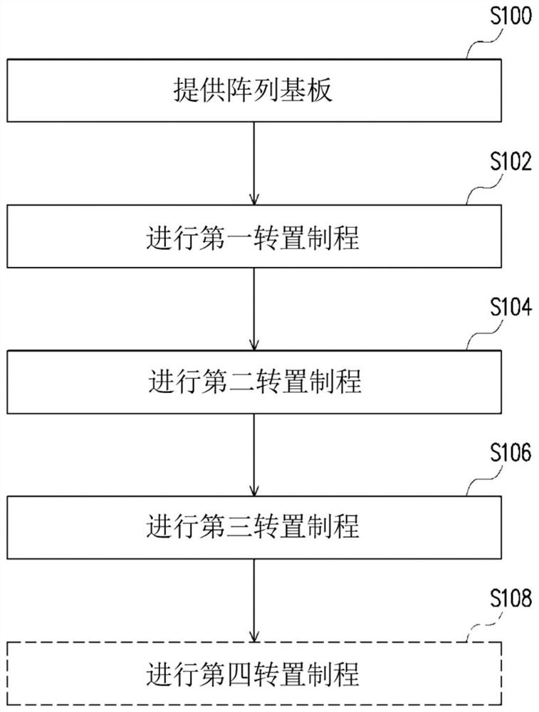
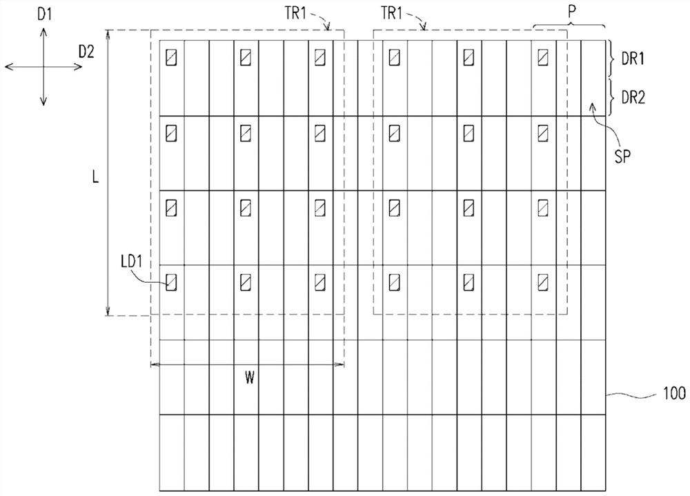
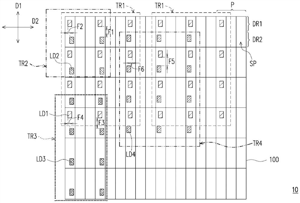
[0046] figure 1 is a flowchart of a manufacturing method of a display device according to some embodiments of the present invention. Figure 2A and Figure 2B It is a schematic top view of different stages in the transposition process of the manufacturing method of the display device according to some embodiments of the present invention. The manufacturing method of the display device according to the embodiment of the present invention includes the following steps.

[0047] Please refer to figure 1 and Figure 2A , proceed to step S100 to provide an array substrate 100 . The material of the array substrate 100 may include glass, ...


PUM

PropertyMeasurementUnit
sizeaaaaaaaaaa

Abstract

The present invention provides a display device and a manufacturing method thereof. The manufacturing method of the display device includes the following steps. Array substrates are provided. The array substrate includes a plurality of sub-pixel areas, and each sub-pixel area includes first and second component areas. A first transposition process is performed to respectively place N first light-emitting elements in the first element regions of the N sub-pixel regions by using the first carrier. A second transposition process is performed to respectively place X second light-emitting elements in the second element regions of the X sub-pixel regions through the second carrier. A third transposition process is performed to respectively place Y second light-emitting elements in the second element regions of the Y sub-pixel regions by using the third carrier. The X sub-pixel regions do not overlap with the Y sub-pixel regions, and the N sub-pixel regions partially overlap with the X sub-pixel regions and the Y sub-pixel regions respectively.

Description

technical field [0001] The present invention relates to a display device and its manufacturing method, and in particular to a light-emitting diode display device and its manufacturing method. Background technique [0002] Light-emitting diodes have the advantages of high energy conversion efficiency, short response time, and long service life. Therefore, in recent years, light-emitting diodes have become the main lighting source with both power saving and environmental protection features. Furthermore, due to the breakthrough in the size of the LED, a technology of micro LED display (micro LED display) that directly places the LED in the pixel structure gradually appears on the market. [0003] The method of transposing the LEDs from the wafer to the array substrate may include stamp imprinting or electrostatic imprinting. Generally speaking, multiple transposition steps are required to place LEDs in all pixels (sub-pixels). The current transposition process includes disp...

Claims


Application Information

Patent Timeline
Patent Type & Authority Patents(China)
IPC IPC(8): H01L21/683H01L25/075
CPCH01L21/6835H01L25/0753H01L2221/68363
Inventor 陈振彰刘品妙杨文玮
Owner AU OPTRONICS CORP
Features
  • R&D
  • Intellectual Property
  • Life Sciences
  • Materials
  • Tech Scout
  • Unparalleled Data Quality
  • Higher Quality Content
  • 60% Fewer Hallucinations
Learn More