Pixel structure
A pixel structure and pixel electrode technology, applied in nonlinear optics, instruments, optics, etc., can solve problems such as uneven brightness of liquid crystal displays, and achieve good display quality, consistent brightness and penetration
- Summary
- Abstract
- Description
- Claims
- Application Information
AI Technical Summary
Problems solved by technology
Method used
Image

Examples
Embodiment Construction
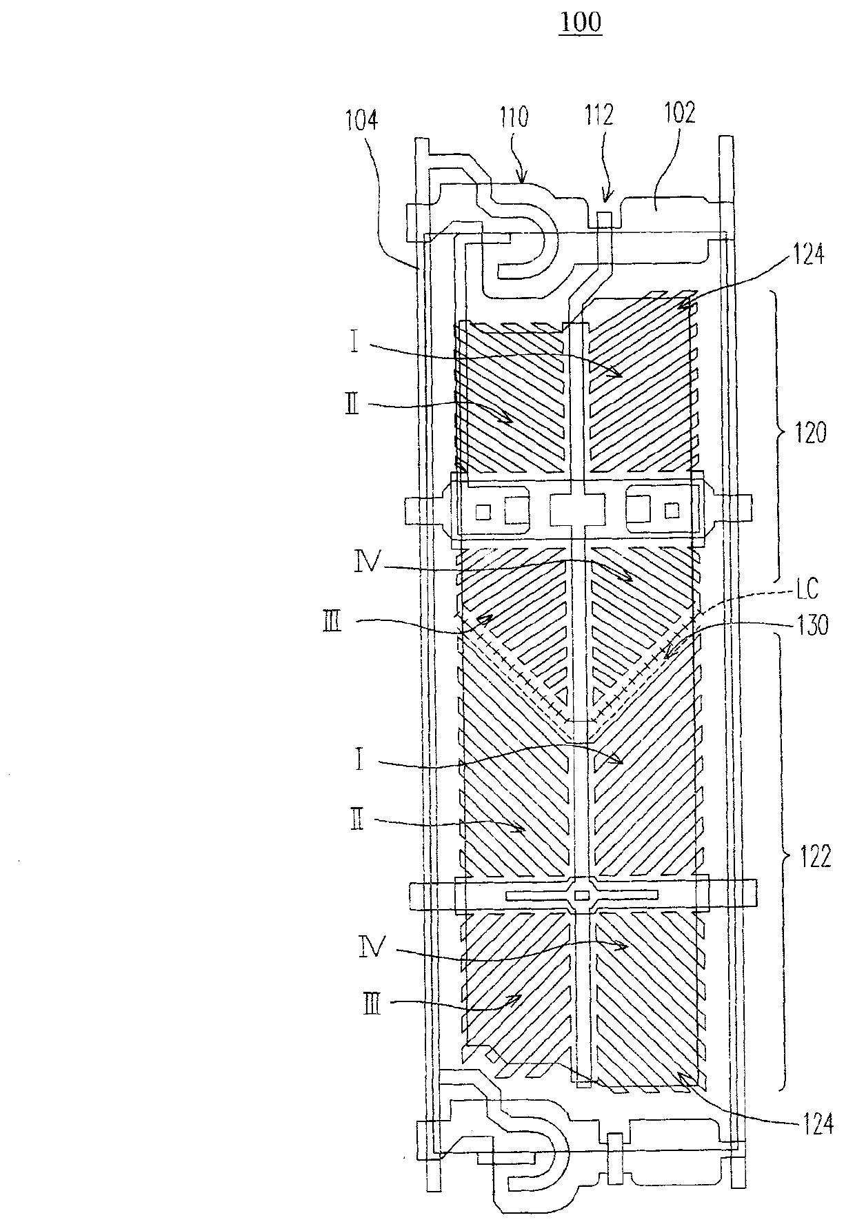
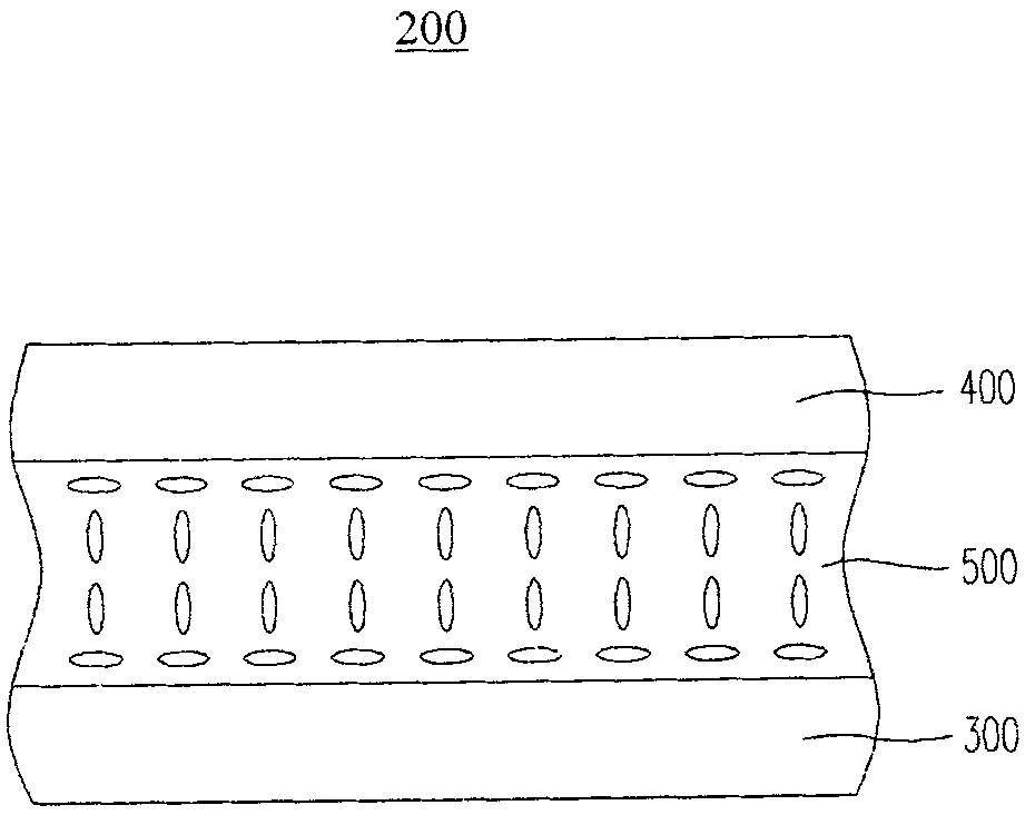
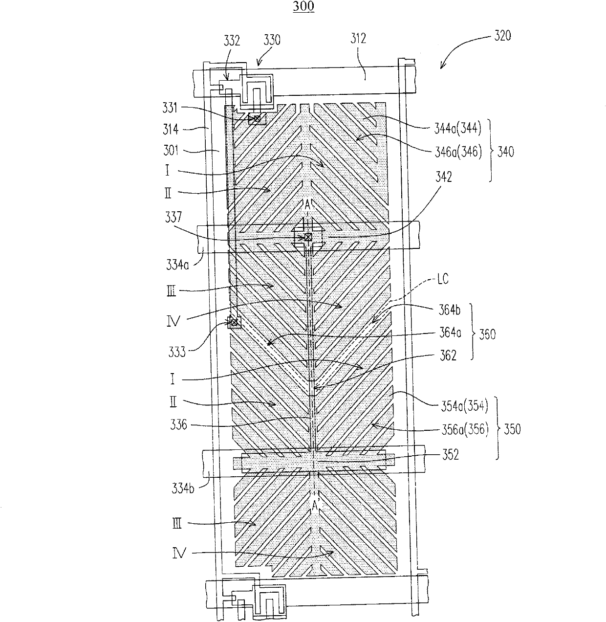
[0025] Figure 2A It is a schematic cross-sectional view of a liquid crystal display according to an embodiment of the present invention. Figure 2B for Figure 2A The partial top view schematic diagram of the active element array substrate of , for the convenience of description, Figure 2B Only one of the pixel structures is shown as a representative. Please also refer to Figure 2A and Figure 2B , the liquid crystal display 200 includes an active device array substrate 300 , an opposite substrate 400 and a liquid crystal layer 500 . The active device array substrate 300 includes a plurality of scan lines 312 , a plurality of data lines 314 and a plurality of pixel structures 320 , wherein each pixel structure 320 is electrically connected to a corresponding data line 312 and a corresponding scan line 314 . The liquid crystal layer 500 is disposed between the active device array substrate 300 and the opposite substrate 400 . The opposite substrate 400 is, for example,...
PUM
 Abstract
Description
Claims
Application Information
 - R&D
- Intellectual Property
- Life Sciences
- Materials
- Tech Scout
- Unparalleled Data Quality
- Higher Quality Content
- 60% Fewer Hallucinations
Browse by: Latest US Patents, China's latest patents, Technical Efficacy Thesaurus, Application Domain, Technology Topic, Popular Technical Reports.
© 2025 PatSnap. All rights reserved.Legal|Privacy policy|Modern Slavery Act Transparency Statement|Sitemap|About US| Contact US: help@patsnap.com