Semiconductor device and method for production thereof
A manufacturing method and semiconductor technology, applied in semiconductor/solid-state device manufacturing, semiconductor devices, transistors, etc., can solve problems such as low Ge content, shallow grooves, and compressive strain in hard-to-channel regions
- Summary
- Abstract
- Description
- Claims
- Application Information
AI Technical Summary
Problems solved by technology
Method used
Image

Examples
no. 1 approach
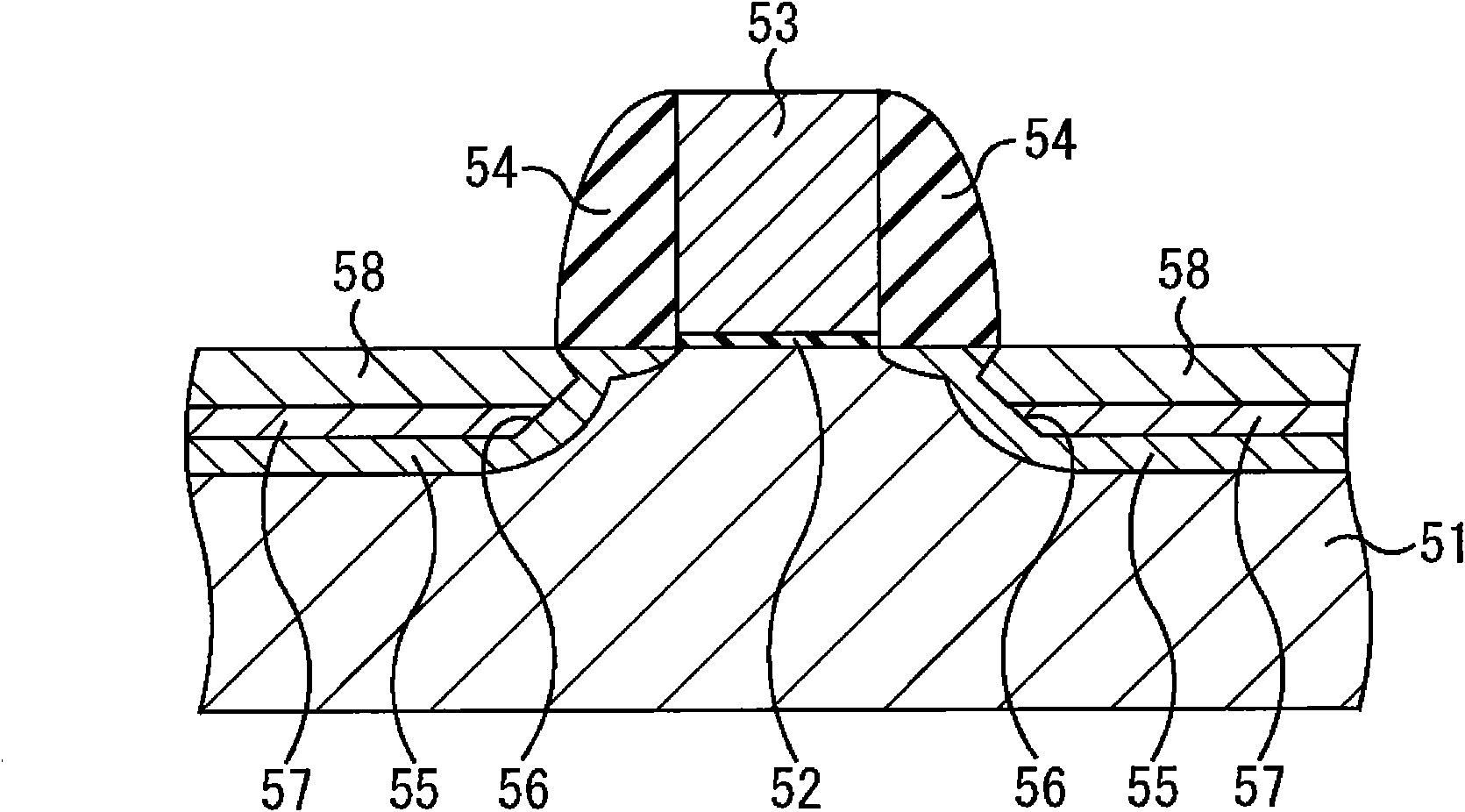
[0054] Next, a first embodiment will be specifically described with reference to the drawings. However, for convenience, the structure of the semiconductor device will be described together with the method of manufacturing the semiconductor device. The first embodiment mainly relates to p-channel MOS transistors. Figure 3A ~ Figure 3M It is a sectional view showing the manufacturing method of the semiconductor device of the first embodiment in order of processes.
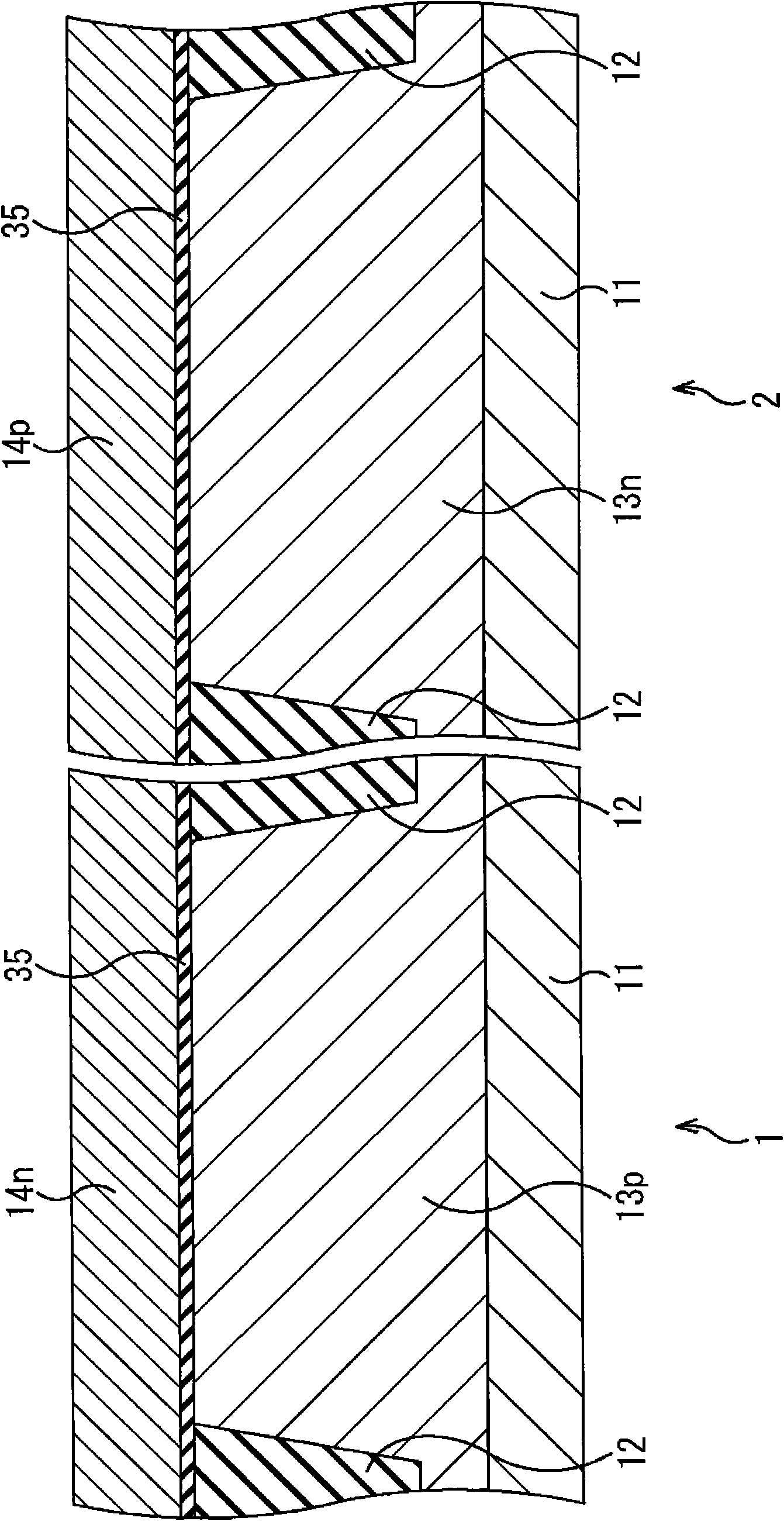
[0055] First, if Figure 3A As shown, on the surface of a p-type silicon substrate 11, an element isolation insulating film 12 for dividing nMOS region 1 and pMOS region 2 is formed by STI (Shallow Trench Isolation: Shallow Trench Isolation) method. The nMOS region 1 is a region where an n-channel MOS transistor is to be formed, and the pMOS region 2 is a region where a p-channel MOS transistor is to be formed. When the element isolation insulating film 12 is formed, first, a silicon oxide film with a thickness ...
no. 2 approach
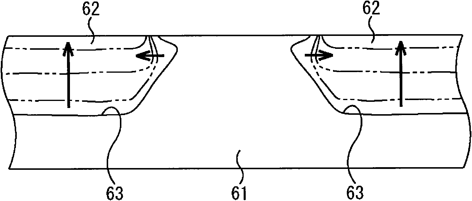
[0081] Next, a second embodiment will be specifically described with reference to the drawings. Wherein, for convenience, the structure of the semiconductor device and the manufacturing method of the semiconductor device will be described together. The second embodiment mainly relates to n-channel MOS transistors. In n-channel MOS transistors, it is necessary to generate lateral tensile strain in the channel region. For this purpose, for example, it is only necessary to form a SiC layer in the groove. In addition, by appropriately controlling the C content when forming the SiC layer, the same effect as that of the first embodiment can be obtained also in the n-channel MOS transistor. Figure 9A ~ Figure 9E It is a cross-sectional view showing the manufacturing method of the semiconductor device according to the second embodiment in order of steps.
[0082] First, in the same manner as in the first embodiment, the processes up to the formation of the silicon oxide film 18 an...
PUM
| Property | Measurement | Unit |
|---|---|---|
| Film thickness | aaaaa | aaaaa |
| Thickness | aaaaa | aaaaa |
| Thickness | aaaaa | aaaaa |
Abstract
Description
Claims
Application Information
 - R&D
- Intellectual Property
- Life Sciences
- Materials
- Tech Scout
- Unparalleled Data Quality
- Higher Quality Content
- 60% Fewer Hallucinations
Browse by: Latest US Patents, China's latest patents, Technical Efficacy Thesaurus, Application Domain, Technology Topic, Popular Technical Reports.
© 2025 PatSnap. All rights reserved.Legal|Privacy policy|Modern Slavery Act Transparency Statement|Sitemap|About US| Contact US: help@patsnap.com