

Manufacturing method of multilayer flexible printed wiring board
A technology of flexible printing and manufacturing method, which is applied in the direction of multi-layer circuit manufacturing, printed circuit, electrical connection formation of printed components, etc.
- Summary
- Abstract
- Description
- Claims
- Application Information
AI Technical Summary
Problems solved by technology
Method used
Image

Examples
Embodiment 1
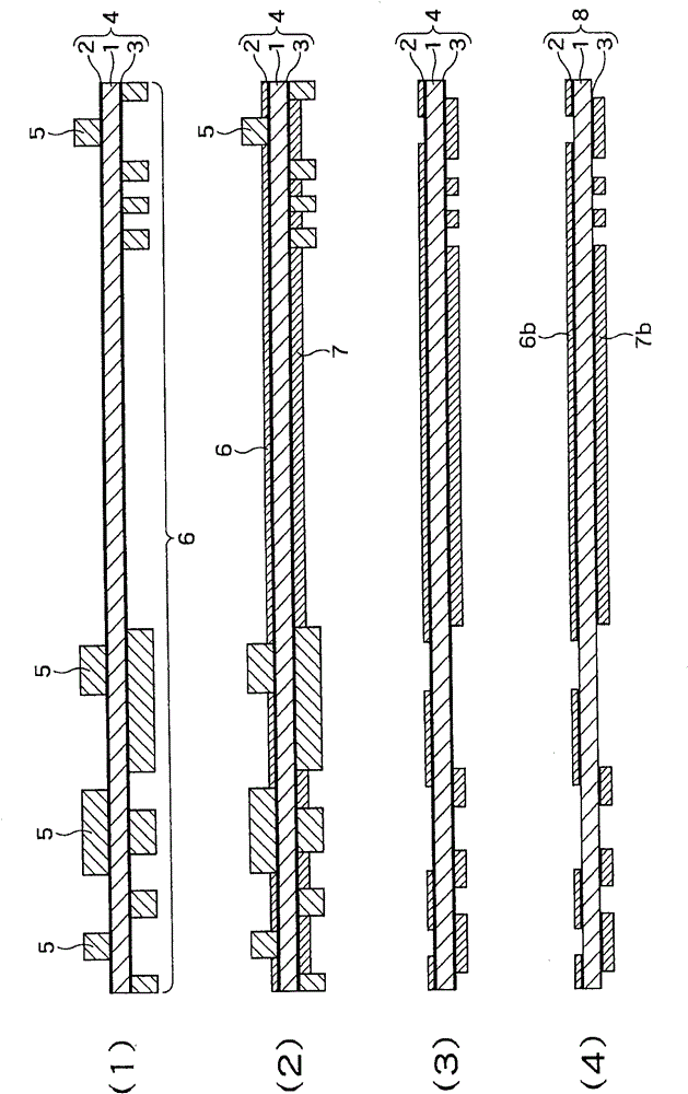
[0049] Figure 1A to Figure 1C It is a sectional structural view showing the manufacturing method of the wiring board of this invention. First, if Figure 1A As shown in (1), prepare a double-sided circuit having copper films 2 and 3 with a thickness of 0.3 μm on both sides of a flexible insulating base material 1 (here, polyimide with a thickness of 12.5 μm) such as polyimide. Base material 4.
[0050] The thickness of the copper thin film is preferably 0.1 to 0.5 μm. When the thickness is less than 0.1 μm, film defects such as pinholes (pinholes) are likely to occur on the copper foil film, which adversely affects the formation of subsequent circuit patterns.
[0051] In addition, when it is thicker than 0.5 μm, when the circuit pattern is formed by a semi-additive method using the copper foil film as a seed layer, and then the seed layer is removed, the film of the circuit pattern is reduced due to etching and removal for each circuit pattern. If it is too large, the st...
PUM
 Abstract
Description
Claims
Application Information