Method for calibrating sensing brightness of image sensor

An image sensor and brightness technology, applied in the input/output process of instruments, data processing, electrical digital data processing, etc., can solve problems such as affecting the sensing brightness and reducing the accuracy of touch operations.

Inactive Publication Date: 2011-03-23
QISDA SUZHOU +1
View PDF4 Cites 4 Cited by
  • Summary
  • Abstract
  • Description
  • Claims
  • Application Information

AI Technical Summary

Problems solved by technology

When the pixel interval corresponding to some image sensors undergoes the whitening process, such as image 3 and Figure 4 When the average luminance (or luminance distribution) of the pixel interval D3 shown is not consistent with other pixel intervals, it will continue to affect the sensing brightness of the optical touch panel, resulting in errors and reducing the accuracy of touch operations.

Method used


Image

  • Method for calibrating sensing brightness of image sensor
  • Method for calibrating sensing brightness of image sensor
  • Method for calibrating sensing brightness of image sensor

Examples


Embodiment Construction

[0028] In order to have a further understanding of the purpose, structure, features, and functions of the present invention, the following detailed descriptions are provided in conjunction with the embodiments.

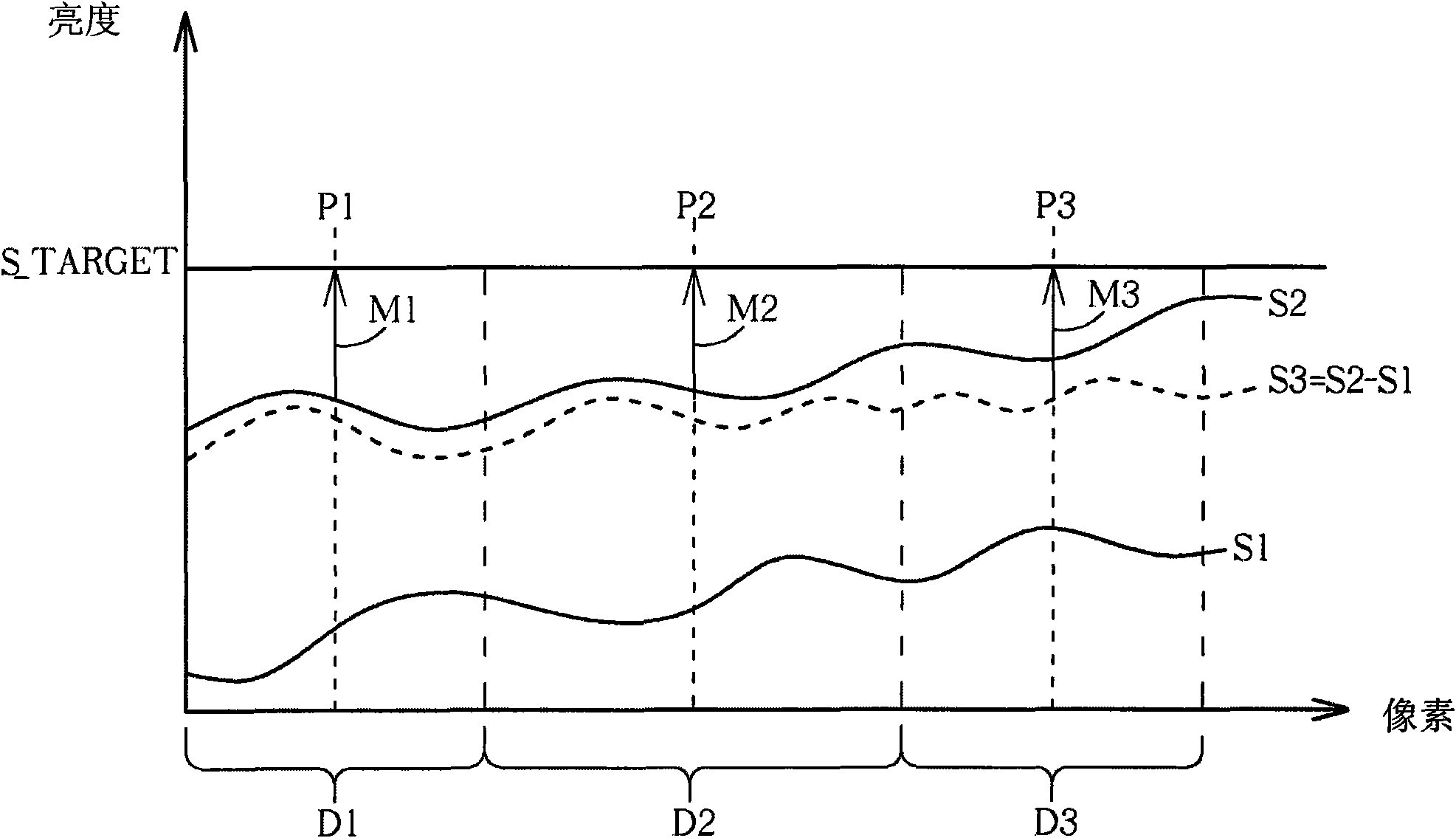
[0029] See Figure 5 and Image 6 . Figure 5 For image 3 When the average brightness of the pixel interval D3 is higher than that of other pixel intervals, the method disclosed in the present invention is implemented to improve the uneven brightness phenomenon. Image 6 For Figure 4 When the average brightness of the pixel interval D3 shown is lower than that of other pixel intervals, the method disclosed in the present invention is implemented to improve the uneven brightness phenomenon.

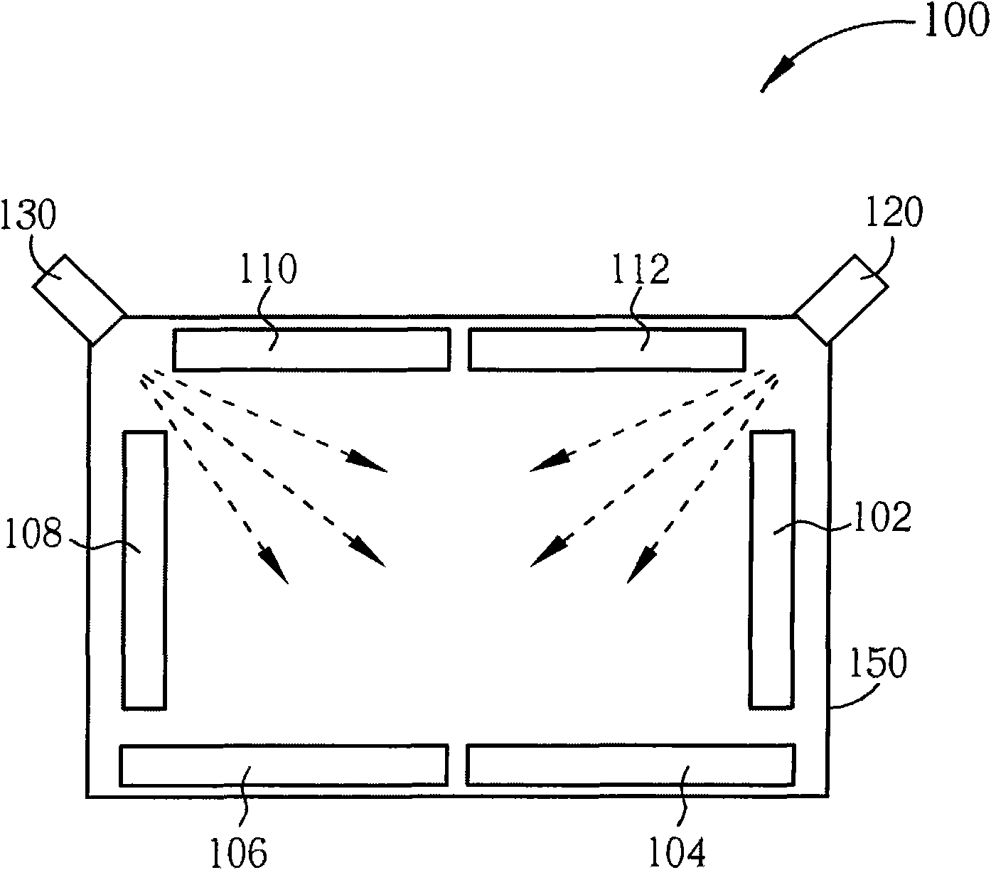
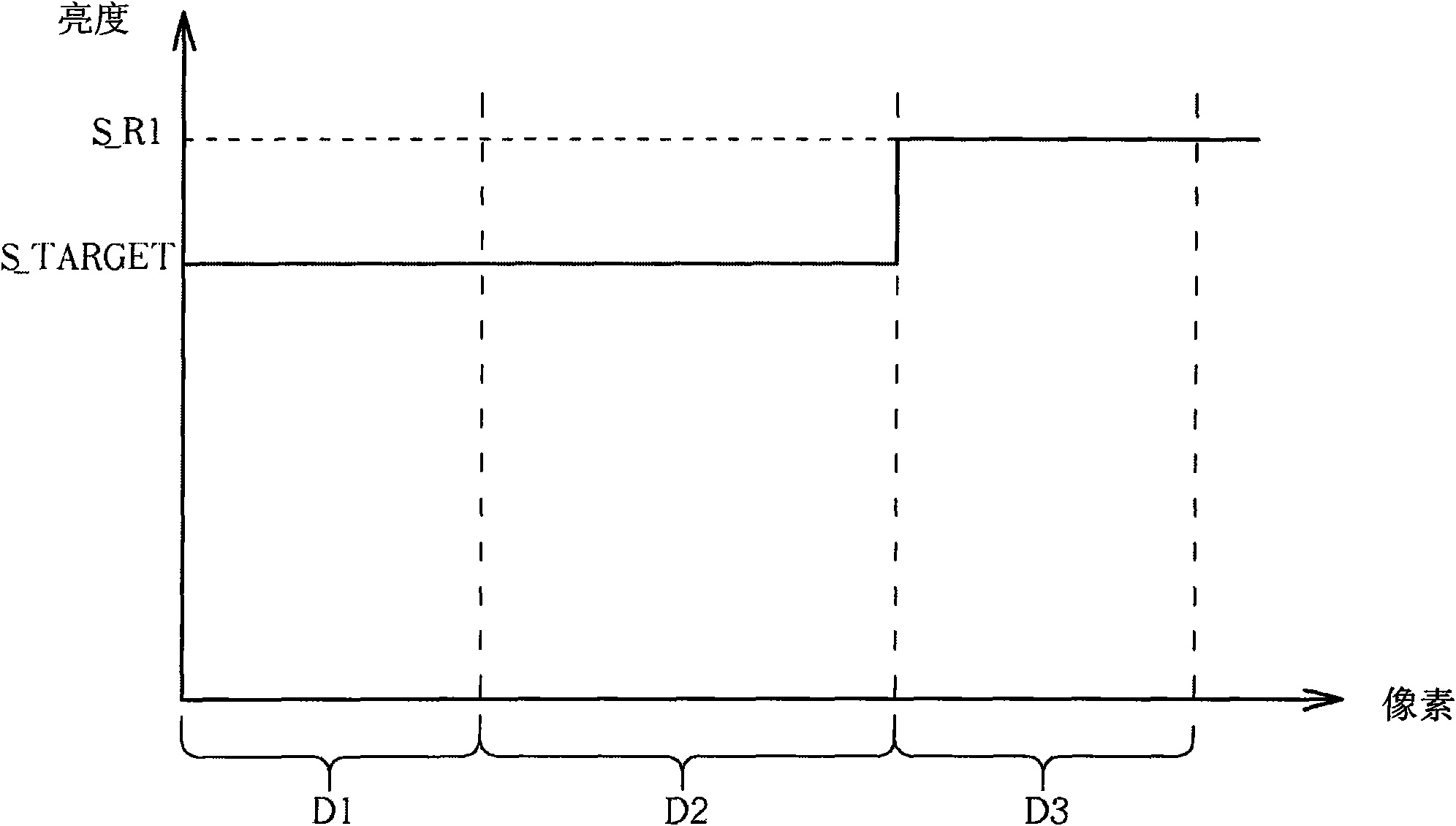
[0030] Such as Figure 5 As shown, in one embodiment, the pixel interval D3 is an image generated by the image sensor according to the light source 108. When the current average brightness S_R1 of the pixel interval D3 is higher than the reference brightness S_TARGET, it indicates that...


PUM


Abstract

The invention provides a method for calibrating the sensing brightness of an image sensor. In the method, after the image sensor in an optical touch panel is subject to a whitening program to calibrate the sensing brightness, the brightness distribution after whitening is multiplied by a brightness multiplying factor, and the brightness distribution after whitening is calibrated to be approximate or equal to a datum brightness to ensure that the brightness distribution after whitening can not be disturbed by external factors and have an error. By adopting the method, the phenomenon of non-uniform brightness caused by larger brightness distribution gap generated in the detection range of the image sensor can be solved.

Description

Technical field [0001] The invention discloses a method for calibrating the sensing brightness of an image sensor, in particular to a method for performing calibration again to compensate for errors caused by external factors after performing a whitening procedure to calibrate the image sensor. Background technique [0002] Generally, in a touch device equipped with an optical touch panel, at least one set of image sensors are arranged on the optical touch panel to detect any effective touch behavior of the user on the optical touch panel, and make The touch device can respond to the touch command sent by the user to the optical touch panel accordingly. [0003] See figure 1 , Which is a schematic diagram of the interior of an optical touch panel with an image sensor. Such as figure 1 As shown, the optical touch panel 100 has a body 150 and image sensors 120 and 130. The main body 150 has a plurality of light source modules 102, 104, 106, 108, 110, 112, and the image sensors 120,...

Claims


Application Information

Patent Timeline
Patent Type & Authority Applications(China)
IPC IPC(8): G06F3/042
Inventor 黄祺钦张皓崴李俊仁
Owner QISDA SUZHOU
Why Eureka
Try Eureka