Method for driving display

A driving method and display technology, applied in static indicators, instruments, semiconductor lamps, etc., can solve problems such as uneven brightness, critical voltage shift of thin film transistors, etc.

Active Publication Date: 2006-12-06
AU OPTRONICS CORP
View PDF0 Cites 4 Cited by
  • Summary
  • Abstract
  • Description
  • Claims
  • Application Information

AI Technical Summary

Problems solved by technology

[0010] In view of the above-mentioned problems caused by the driving method of the existing active display, the present invention proposes an electroluminescent display driving method to solve the problem of critical voltage drift of thin-film tran

Method used


Image

  • Method for driving display
  • Method for driving display
  • Method for driving display

Examples


Embodiment Construction

[0042] The "electroluminescence display and its driving method" of the present invention is described in detail with the drawings, and the preferred

[0043] Embodiment description is as follows:

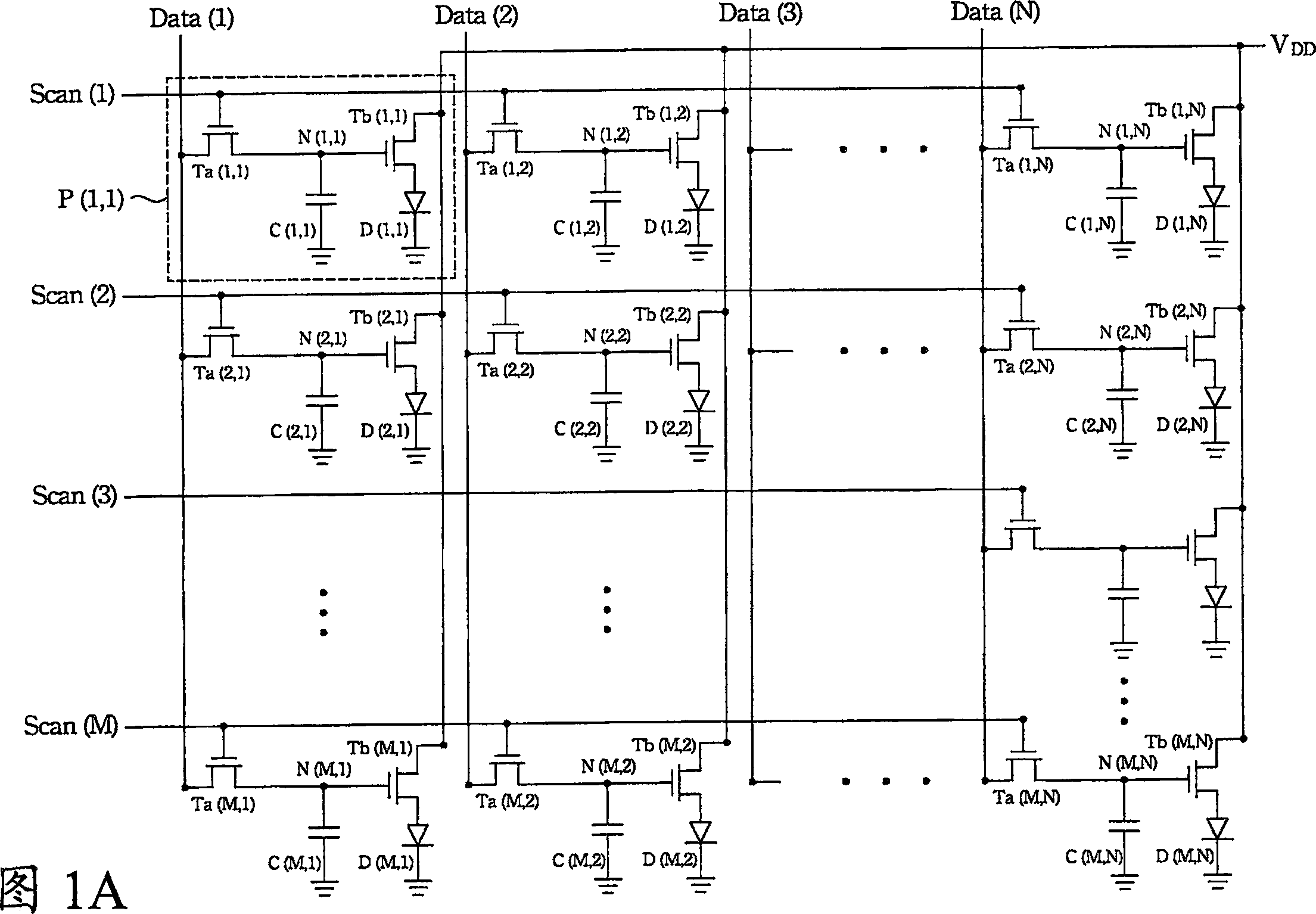
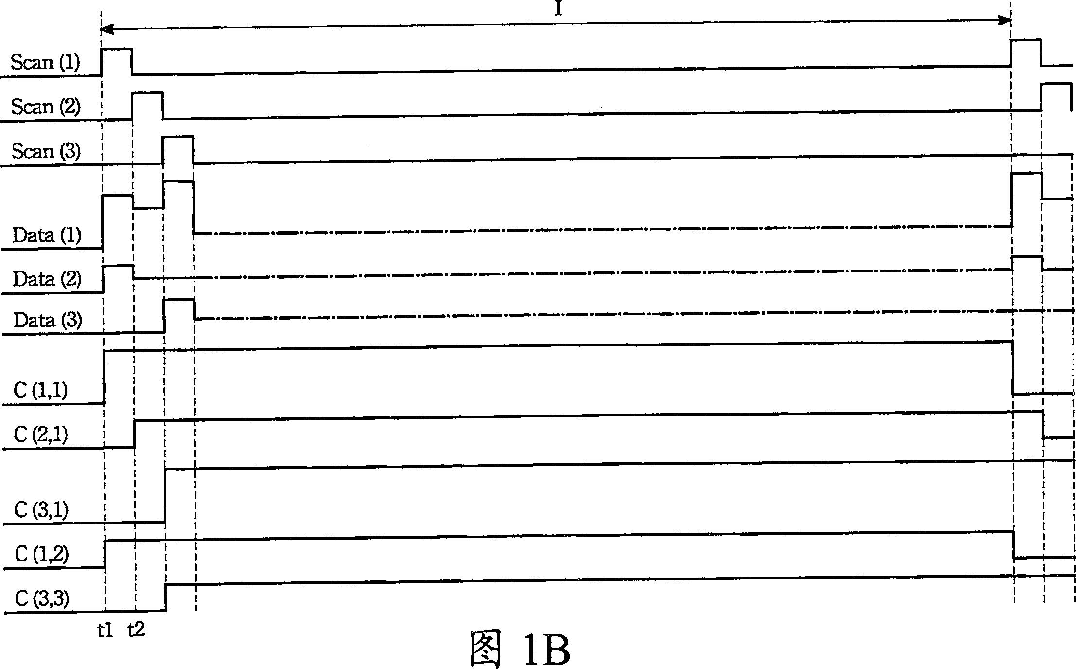
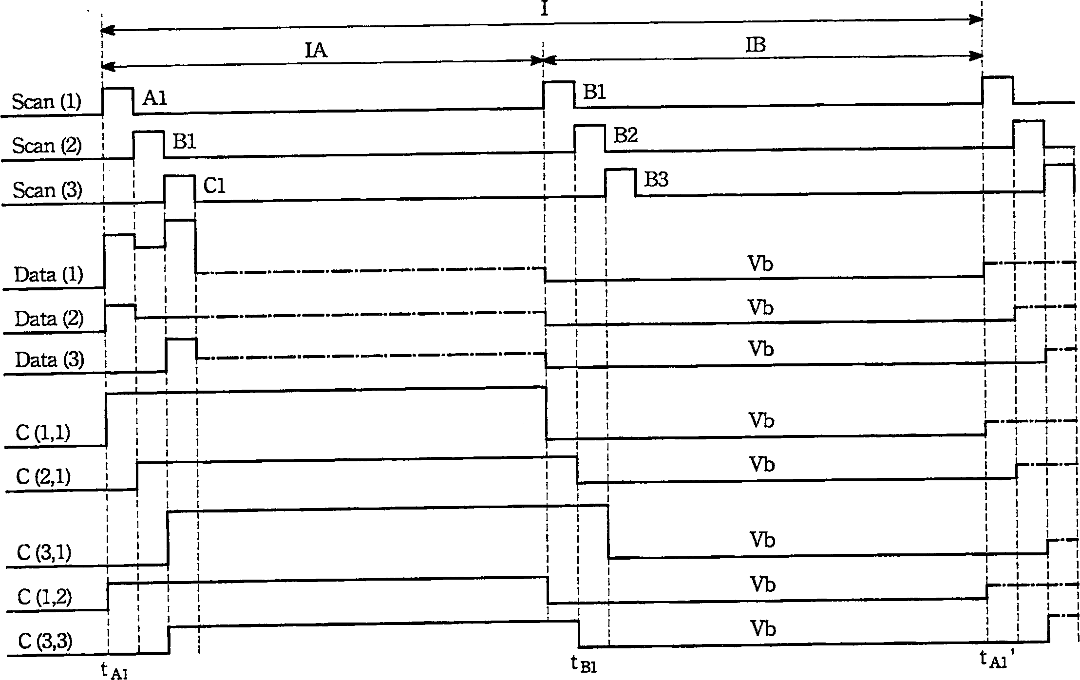
[0044] In the electroluminescence display of the present invention, the circuit diagram of the OLED pixel array and its pixel structure are shown in FIGS. 2A-2B . The electroluminescent display has M scanning lines Scan, N data lines Data and a pixel array of M columns and N rows. The pixel array has M×N pixels for displaying a frame in a display period. Each pixel P has a switching transistor Ta, a driving transistor Tb, a light emitting unit D and a capacitor C. As shown in FIG. The source S and the gate G of the switch transistor Ta are respectively connected to a data line Data and a scan line Scan. The drain and source S of the driving transistor Tb are respectively electrically connected to a display voltage source V DD And the light emitting unit D, the gate G of which is...


PUM


Abstract

The invention is a driving method for a display device, applied to an electrically lighting display device which has plural pixel columns, where each pixel comprises a lighting cell, a switch transistor and a drive transistor connected to the switch transistor and the lighting cell. And the driving method controls the electrically lighting display device to display a frame picture in a display period and comprises the steps of: defining the display period which has three time intervals; in order starting up the pixel columns in the first and second time intervals; providing a displayed data for the pixel columns in the first time interval; providing a gray level data for the pixel columns in the second time interval; and resetting the pixel columns in the third time interval.

Description

technical field [0001] The present invention relates to a driving method of a display, in particular to a driving method of an electroluminescent display with a thin film transistor electrical reset program. Background technique [0002] The organic light emitting diode is a current-driven element, and its luminous brightness changes with the current passing through the organic light emitting diode. Active devices of OLEDs include polysilicon thin film transistors (LTPS-TFTs) and amorphous silicon thin film transistors (a-Si TFTs). Among them, polysilicon thin-film transistors are more commonly used in the industry today; amorphous silicon thin-film transistors will become the future trend because of the small number of masks required for its manufacturing process, low film forming temperature and low cost. However, whether it is a polysilicon thin film transistor or an amorphous silicon thin film transistor, there is a problem that the threshold voltage value rises to caus...

Claims


Application Information

Patent Timeline
IPC IPC(8): G09G3/30G09G3/32H05B33/08G09G3/3258H05B44/00
CPCY02B20/346Y02B20/30
Inventor 唐宇骏叶政男
Owner AU OPTRONICS CORP
Why Eureka
Try Eureka