Dimmer lighting assembly and manufacturing method thereof
A technology of light-emitting components and manufacturing methods, which is applied to optical elements, light sources, electric light sources, etc. used to change the spectral characteristics of emitted light, and can solve problems such as not being economical, cost-intensive, and unable to coat light-emitting diode chips. Achieve the effect of increasing the diversity of luminous colors and reducing the probability of failure
- Summary
- Abstract
- Description
- Claims
- Application Information
AI Technical Summary
Problems solved by technology
Method used
Image

Examples
Embodiment Construction
[0043] The invention discloses a dimming light-emitting component, which has wide applicability. In order to make the narration of the present invention more detailed and complete, refer to the following description and cooperate Figure 1 to Figure 4 attached drawings.
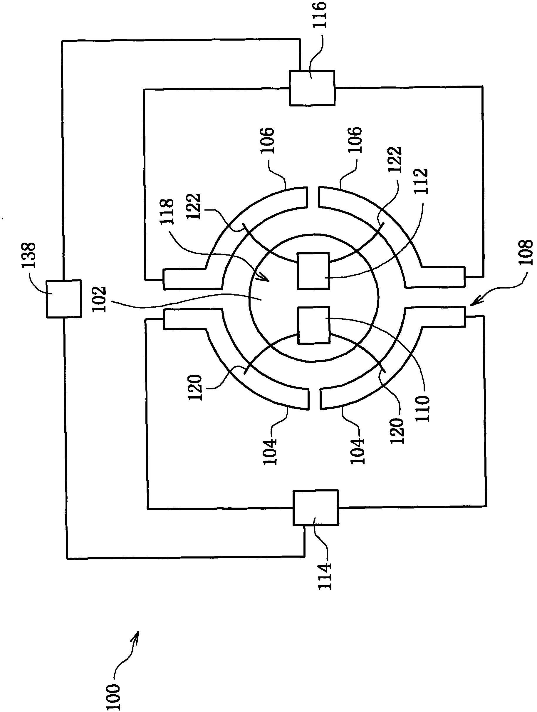
[0044] Please refer to figure 1 , which is a schematic top view showing a dimming light-emitting component according to an embodiment of the present invention. In one embodiment, the dimming light-emitting component 100 mainly includes a bracket 108 , at least two light-emitting chips 110 and 112 , and at least two independent power sources 114 and 116 . The independent power sources 114 and 116 are respectively electrically connected to the corresponding light-emitting chips 110 and 112 to supply the required power.
[0045] In one embodiment, the bracket 108 includes a chip carrier 102 and at least two pairs of pins 104 and 106 .
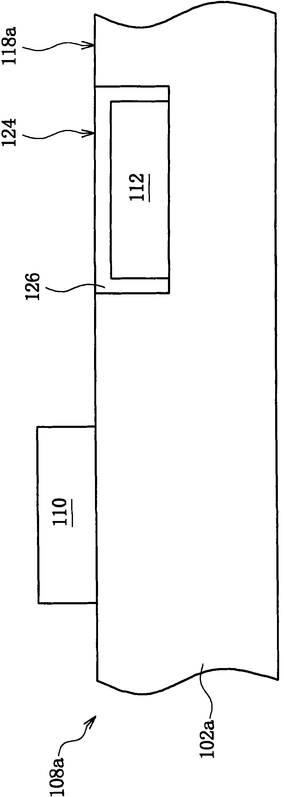
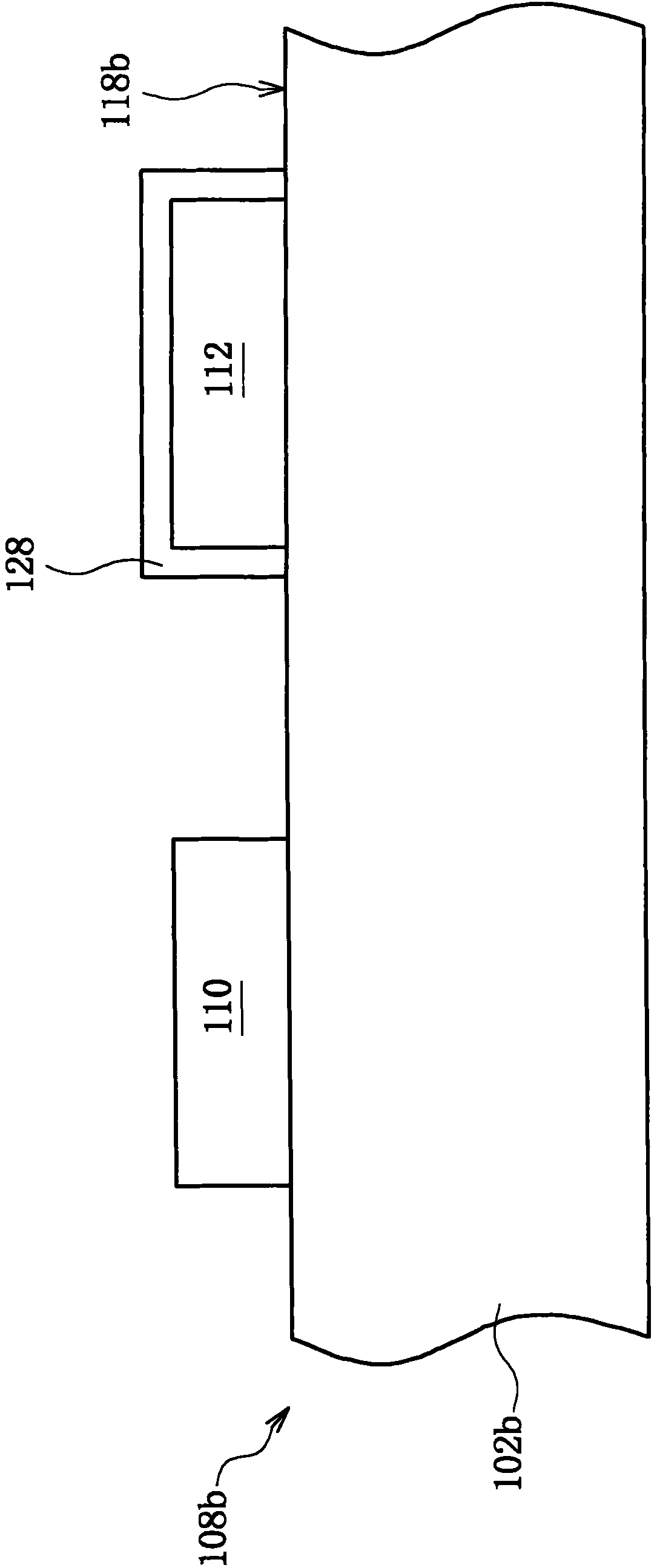
[0046] Please refer to figure 2 , which is a cross-sectional view of p...
PUM
 Abstract
Description
Claims
Application Information
PatSnap Eureka turns technology decisions into work you can execute. Powered by our Innovation Knowledge Graph, it runs expert workflows across engineering, life sciences, materials and intellectual property. Get your review-ready output in minutes.


