

Capacitive touch structure, manufacturing method thereof and touch equipment
A technology of capacitive touch and manufacturing method, which is applied in the direction of electrical digital data processing, instrumentation, input/output process of data processing, etc., can solve the problems such as the reduction of the display effect of the display, and achieve the effect of improving the light transmittance
- Summary
- Abstract
- Description
- Claims
- Application Information
AI Technical Summary
Problems solved by technology
Method used
Image

Examples
Embodiment Construction
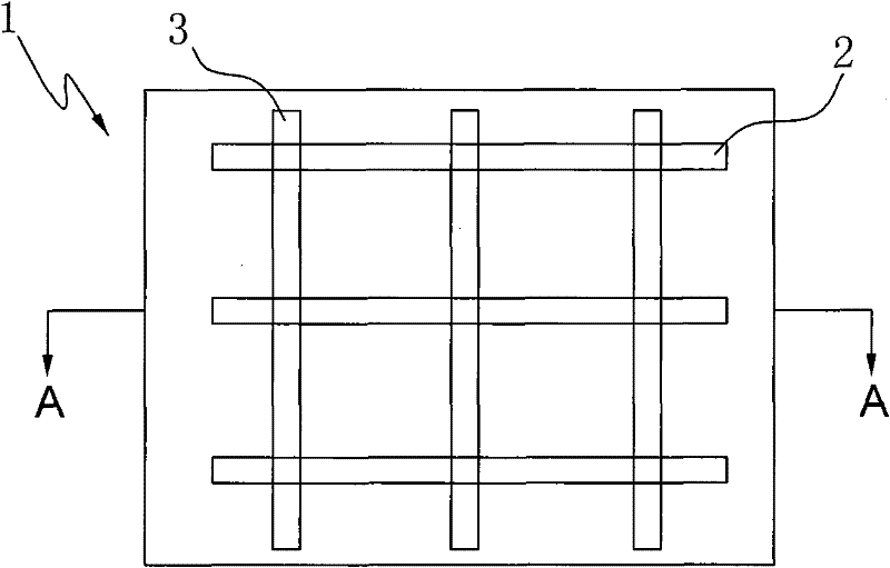
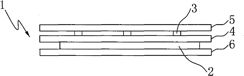
[0049] The capacitive touch structure of the present invention includes a substrate, a first direction electrode arranged on the surface of the substrate, an insulating layer arranged on the surface of the first direction electrode, and a second direction electrode arranged on the surface of the insulating layer facing away from the first direction electrode The electrodes in the first direction and the electrodes in the second direction are intersected with each other and separated by an insulating layer. The capacitive touch structure further includes a protection block, which is arranged on the surface of the electrodes in the second direction and only covers the electrodes in the second direction and the electrodes in the first direction. The intersection of electrodes to achieve the purpose of saving protective layer materials.
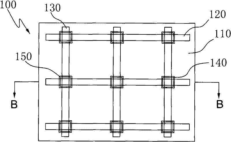
[0050] Such as image 3 , 4 As shown, the capacitive touch structure 100 according to the first embodiment of the present invention includes a ...
PUM
 Abstract
Description
Claims
Application Information