

Solar cell and preparation method thereof
A solar cell and electrode technology, applied in circuits, photovoltaic power generation, electrical components, etc., can solve the problems of grid shading and high resistivity, and achieve the effects of improving conversion efficiency, improving quality, and improving short-circuit current.
- Summary
- Abstract
- Description
- Claims
- Application Information
AI Technical Summary
Problems solved by technology
Method used
Image

Examples
preparation example Construction
[0064] A method for preparing a solar cell provided by an embodiment of the present invention includes the following steps:
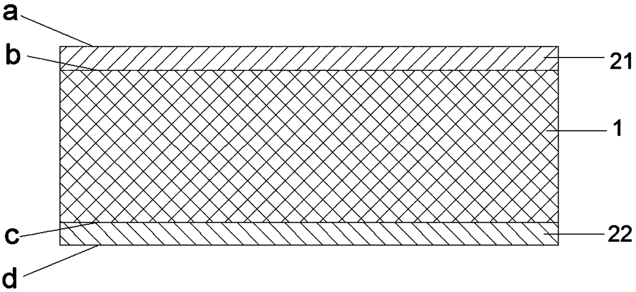
[0065] A first electrode 21 is formed on the light-receiving side of the power generation body 1; a second electrode 22 is formed on the backlight side of the power generation body 1; wherein, the first electrode 21 includes a first graphene layer.
[0066] In the embodiment of the present invention, the power generating body 1 is obtained by a conventional preparation method, which will not be repeated here. Preferably, the power generation body 1 is a silicon heterojunction power generation body or a perovskite power generation body.
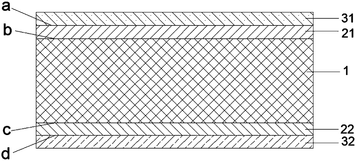
[0067] Further, the second electrode 22 includes a second graphene layer, a transparent conductive oxide layer or a metal layer; the embodiment of the present invention does not specifically limit the preparation method of the transparent conductive oxide layer or the metal layer, preferably, transparent conductive oxid...
Embodiment 1
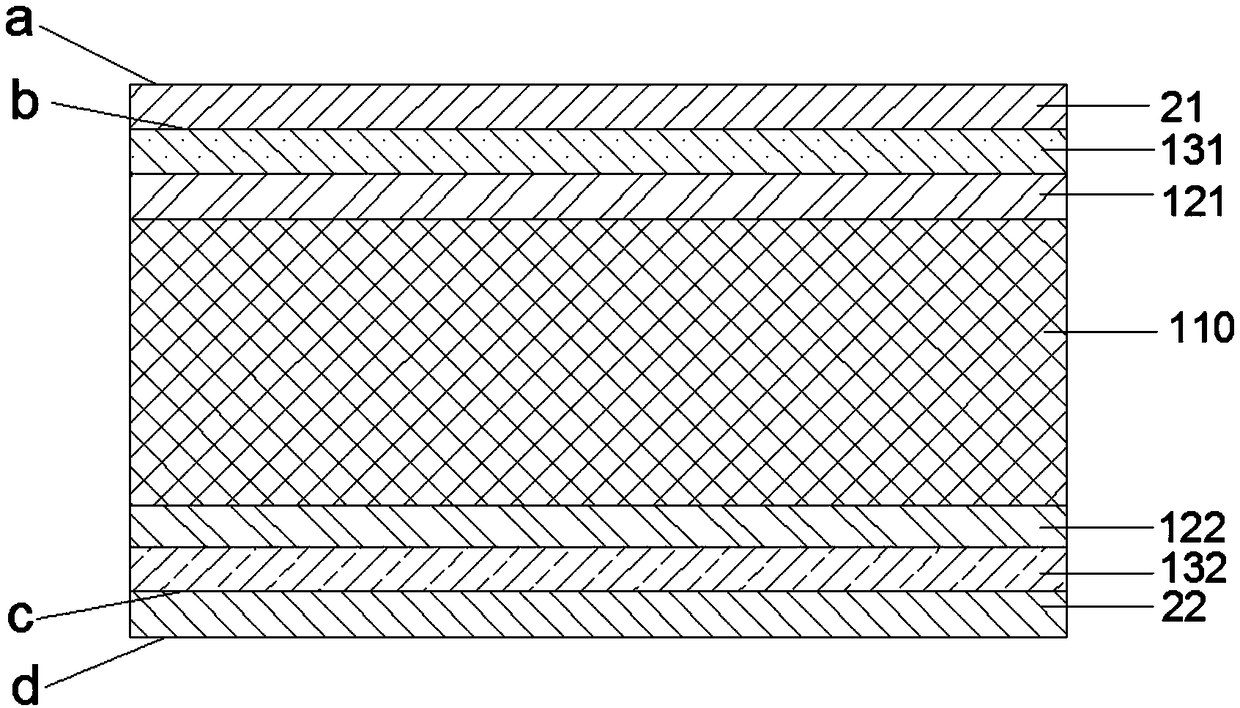
[0084] A silicon heterojunction solar cell, such as image 3 As shown, it includes: an electrode body 1, a first electrode 21 and a second electrode 22, wherein the electrode body 1 includes in sequence from bottom to top: a P-type amorphous silicon doped layer 132, a second intrinsic layer of amorphous silicon 122 , an N-type silicon wafer 110 , a first intrinsic layer of amorphous silicon 121 and an N-type doped layer of amorphous silicon 131 .
[0085] The first electrode 21 is a first graphene layer, which is arranged on the upper surface of the N-type amorphous silicon doped layer 131;
[0086] The second electrode 22 is a second graphene layer disposed on the lower surface of the P-type amorphous silicon doped layer 132 .
[0087] The thickness of the N-type silicon wafer 110 is 120um, the thickness of the first amorphous silicon intrinsic layer 121 is 10nm, the thickness of the second amorphous silicon intrinsic layer 122 is 10nm, and the thickness of the N-type amorph...
Embodiment 2
[0090] A silicon heterojunction solar cell, such as Figure 4 Shown, its preparation method comprises the steps:
[0091] (1) Preparation of electrode body 1:
[0092] The electrode body 1 is manufactured by a conventional method, and the electrode body 1 is a heterojunction electrode body, which includes from bottom to top: a P-type amorphous silicon doped layer 132, a second amorphous silicon intrinsic layer 122, an N-type silicon A sheet 110, a first intrinsic layer of amorphous silicon 121 and an N-type doped layer of amorphous silicon 131;
[0093] (2) Preparation of the first electrode 21:
[0094] The first electrode 21 is prepared by a gallium-catalyzed chemical vapor deposition method, which specifically includes the following steps:
[0095] a. In the first chamber, gallium metal is used as a catalyst, and gallium is heated to 1200°C in a vacuum state, and 1 sccm of methane and 250 sccm of 6N argon are introduced for 300 seconds; methane is decomposed into carbon ...
PUM
| Property | Measurement | Unit |
|---|---|---|
| Thickness | aaaaa | aaaaa |
| Thickness | aaaaa | aaaaa |
| Thickness | aaaaa | aaaaa |
Abstract
Description
Claims
Application Information