Circuit board manufacturing method

A technology of circuit board production and copper-clad substrate, which is applied in the direction of removing conductive materials by chemical/electrolytic methods, and can solve problems such as image sensor deviation, photomask and circuit board alignment deviation, and circuit board scrapping. Achieve accurate alignment, improve signal transmission quality, and prevent excessive alignment errors

Inactive Publication Date: 2012-02-08
AVARY HLDG (SHENZHEN) CO LTD +1
View PDF5 Cites 17 Cited by
  • Summary
  • Abstract
  • Description
  • Claims
  • Application Information

AI Technical Summary

Problems solved by technology

However, in the first alignment method, the photoresist formed on the circuit board may not completely cover the alignment copper block. Due to the refraction of light by the photoresist, the alignment copper obtained by the image sensor The image of the block will have different degrees of deformation in the area with or without photoresist, so that the image sensor will deviate when determining the virtual center of the alignment copper block, resulting in the alignment of the photomask and the circuit board deviation
In the second alignment method, part of the photoresist on the circuit board may enter the alignment hole, and part of the l...

Method used


Image

  • Circuit board manufacturing method
  • Circuit board manufacturing method
  • Circuit board manufacturing method

Examples


Embodiment Construction

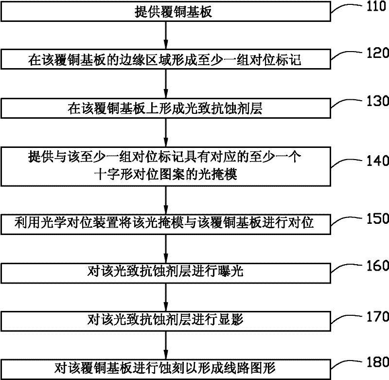
[0054] The circuit board manufacturing method of the technical solution will be further described in detail below in conjunction with the accompanying drawings and embodiments.

[0055] see figure 1 , the embodiment of the technical solution provides a circuit board manufacturing method, which includes the following steps:

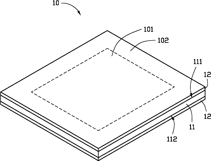
[0056] Step 110, see figure 2 , providing a copper clad substrate 10 .

[0057] In this embodiment, the copper clad substrate 10 includes a first insulating layer 11 and a first copper foil layer 12 . The first insulating layer 11 has a first surface 111 and a second surface 112 opposite to each other. The first surface 111 is parallel to the second surface 112 . A first copper foil layer 12 is disposed on the first surface 111 and the second surface 112 respectively, that is, the copper clad substrate 10 is a double-sided board. Of course, the copper-clad substrate 10 can also be a single-sided board with only one first copper foil layer 12 . The c...


PUM


Abstract

The invention relates to a circuit board manufacturing method, which comprises the following steps: a copper-clad substrate is provided, wherein the copper-clad substrate is provided with a molding area and an edge area surrounding the molding area; at least one group of counterpoint marks are formed at the edge area of the copper-clad substrate, wherein each group of counterpoint marks include a plurality of marks distributed crisscross; a photoresist layer is formed on the copper-clad substrate; a photomask is provided, wherein the photomask is provided with at least one cross counterpoint pattern corresponding to at least one group of counterpoint marks; counterpoint is carried out on the photomask and the copper-clad substrate by an optical counterpoint device so as to make at least one cross pattern of the photomask respectively cover at least one group of counterpoint marks of the copper-clad substrate; the photoresist layer is exposed; the photoresist layer is developed; and the copper-clad substrate is etched so as to form a circuit graph on the molding area.

Description

technical field [0001] The invention relates to circuit board technology, in particular to a method for manufacturing a circuit board. Background technique [0002] With the rapid development of the electronic industry, the manufacturing technology of circuit boards, which are the basic components of electronic products, is becoming more and more important. Circuit boards are generally made of copper-clad substrates through a series of processes such as cutting, drilling, exposure, development, etching, lamination, and molding. For details, please refer to the article "Dielectric characterization of printed circuit board substrates" published by C.H.Steer et al. in Proceedings of the IEEE, Vol.39, No.2 (August 2002). [0003] Among them, in the manufacturing process of the circuit board, the exposure step of the circuit board is very important. The accuracy of alignment between the mask and the circuit board during exposure directly affects the accuracy of the subsequently...

Claims


Application Information

Patent Timeline
IPC IPC(8): H05K3/06
Inventor 林钊文
Owner AVARY HLDG (SHENZHEN) CO LTD
Why Eureka
Try Eureka