A flip-chip packaging product without conductive adhesive and its manufacturing process

A technology of chip packaging and manufacturing process, which is applied in semiconductor/solid-state device manufacturing, circuits, electrical components, etc., can solve the problems of large thickness, high cost, and expensive material cost, and achieve cost reduction, high practicability, and chip reduction cost effect

Active Publication Date: 2020-09-01
ARIZON RFID TECH YANGZHOU
View PDF6 Cites 0 Cited by
  • Summary
  • Abstract
  • Description
  • Claims
  • Application Information

AI Technical Summary

Problems solved by technology

[0004] 1) ACP is a thermosetting adhesive mixed with conductive particles with a very uniform particle size, and requires uniform distribution. This material is very expensive; 2) There are conductive particles in the ACP. When bonding, the chip bump and the antenna metal pin must be precisely aligned , if there is a slight deviation in the upper and lower alignment, the bump will short-circuit with another antenna pin through conductive particles (such as figure 2 shown);
[0005] 3) The bump on the chip is pure gold, thick and expensive

Method used


Image

  • A flip-chip packaging product without conductive adhesive and its manufacturing process
  • A flip-chip packaging product without conductive adhesive and its manufacturing process
  • A flip-chip packaging product without conductive adhesive and its manufacturing process

Examples


Embodiment Construction

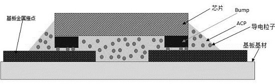
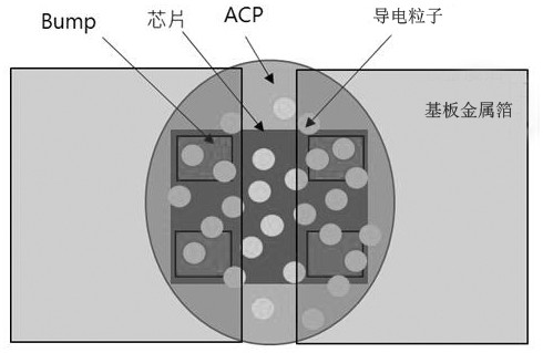
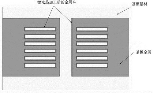
[0029] A flip-chip packaging product that does not use conductive glue, including flip-chip packaging chips and substrates, and the metal foil on the substrate is heated and melted into metal beads. The metal beads are distributed on the substrate contacts and filled between the chip and the substrate. Non-conductive structural glue (thermosetting glue or UV glue), so that the metal beads on the substrate contact or embed on the Bump of the chip or the PAD of the chip.

[0030] The above-mentioned metal beads are made of aluminum, copper, silver, tin, gold-plated copper, tin-plated copper, nickel-plated gold or copper-plated tin-lead.

[0031] The above-mentioned substrates are PET+aluminum flexible substrate, PET+copper flexible substrate, PI+aluminum flexible substrate, PI+copper flexible substrate, FR4+copper substrate, FR4+aluminum substrate, BT+copper substrate or BT+aluminum substrate.

[0032] The Bump or PAD material on the chip above is gold, silver, copper, aluminum,...


PUM

PropertyMeasurementUnit
hardnessaaaaaaaaaa

Abstract

The invention discloses a flip-chip packaging product without conductive glue and a manufacturing process thereof, belonging to the technical field of RFID. The present invention is used in the chip-substrate flip-chip bonding structure, pre-grows metal particles (metal beads) on the substrate as IC chip bump contacts or thick pad contacts (i.e. Bump or PAD), and forms electrical conduction with the substrate contacts The material replaces the conductive particles in the ACP (or ACF) used in the past as the material for the electrical conduction between the chip and the substrate; and then uses a general non-conductive structural adhesive (without conductive particles, non-conductive materials, heat-curable adhesives) or UV-cured glue) to replace the previously used anisotropic conductive glue (ACP or ACF); in terms of process, Flip chip bonding (flip-chip packaging) is used, and a temperature of 140°C-360°C is used during hot pressing.

Description

technical field [0001] The invention relates to a flip-chip packaging product structure without using conductive glue and a manufacturing process thereof, belonging to the technical field of chip packaging. Background technique [0002] Gold bump flip-chip packaging is the bonding of the circuit surface of the chip to the metal circuit surface of the substrate. There are gold bumps (metal bump contacts on the chip, Bump) with a hardness of about 30-120HV on the contact of the circuit surface of the chip. Refers to an unpackaged integrated circuit (IC). Between the chip and the antenna is the anisotropic conductive glue (ACP, which conducts only on the top and bottom of the anisotropic conductive glue, and the glue that is insulated in other directions). This ACP is doped with conductive particles and heat Solid glue. When bonding, the conductive particles harder than the bump are embedded between the bump and the metal foil of the antenna to form a conduction, and the ther...

Claims


Application Information

Patent Timeline
Patent Type & Authority Patents(China)
IPC IPC(8): H01L23/488H01L21/50H01L21/60
CPCH01L21/50H01L23/488H01L24/81H01L2224/81007H01L2224/81095H01L2224/81203H01L21/603H01L2224/73204
Inventor 李宗庭
Owner ARIZON RFID TECH YANGZHOU
Why Eureka
Try Eureka