Supercharge Your Innovation With Domain-Expert AI Agents!

Method for avoiding wafer damage in molding process of wafer level packaging

一种晶圆、工序的技术,应用在晶圆级封装体的制备领域,能够解决晶圆不完全被塑封料覆盖、粘附不佳等问题

Active Publication Date: 2015-04-08
CHONGQING WANGUO SEMICON TECH CO LTD
View PDF5 Cites 0 Cited by
  • Summary
  • Abstract
  • Description
  • Claims
  • Application Information

AI Technical Summary

Problems solved by technology

The technical solution of this patent application is to deal with the problem of poor adhesion between the edge of the wafer and the carrier substrate, but not to the process of plastic sealing the wafer in wafer level packaging
[0008] The field we are concerned about: In the molding process of wafer-level packaging, in terms of reducing the overflow of molding compound, preventing wafer damage, and solving the problem that the edge of the wafer is not completely covered by the molding compound, the above-mentioned patent application scheme or Currently existing technologies are difficult to effectively improve it

Method used


Image

  • Method for avoiding wafer damage in molding process of wafer level packaging
  • Method for avoiding wafer damage in molding process of wafer level packaging
  • Method for avoiding wafer damage in molding process of wafer level packaging

Examples


Embodiment Construction

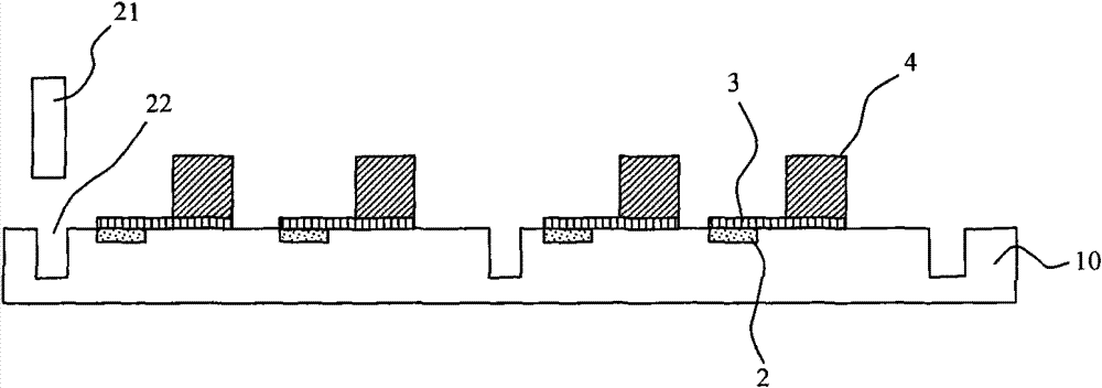
[0049] see image 3 As shown, the front side 100a of the wafer 100 includes a plurality of chips 110, and the plurality of chips 110 are cast and connected to each other. The adjacent chips 110 define the boundaries between each other through the dicing groove 115. Part is edge 120 .

[0050] see Figure 4As shown, in the cross-sectional diagram of the wafer 100 and the chip 110 , the integrated circuit is formed on the front side 100 a of the wafer 100 , and the other side of the wafer 100 is the back side 100 b. The bonding pad (Bond Pad) 101 is used as an input / output contact terminal (I / O Pad) of the internal circuit of the chip 110, and can be a signal input / output, or an interface of Power and Ground. In wafer-level packaging, redistribution technology RDL (Redistribution Technology) can be used to redesign the aluminum pads arranged around the top of the existing chip into a matrix arrangement. In the wafer 100, the top of any chip 110 is provided with a plurality of...


PUM


Abstract

A preparation process of wafer level chip scale packaging that prevents damaging a wafer in molding process is disclosed. In this process, a grinding grove is formed at a top side and around the edge of a wafer before molding is performed. The grinding groove effectively prevents the molding material from overflowing to the edge of the wafer, which avoids the damage of the wafer.

Description

technical field [0001] The present invention generally relates to a method for preparing a wafer-level package, and more precisely, the present invention relates to a method for preventing wafers from being damaged in the plastic sealing process of the wafer-level package during the preparation of the wafer-level package. Methods. Background technique [0002] Different from the traditional chip packaging method, WLCSP (Wafer Level ChipScale Packaging) is packaged and tested on the entire wafer first, and then cut into individual IC particles, so the volume of the package after packaging That is, almost equal to the original size of the bare chip. [0003] Usually, many chips (Die) are separated from the wafer by dicing the wafer (Wafer Saw), and the cutting line of the dicing knife in this process depends on the scribe lines (Scribe Line) arranged on the wafer. [0004] In the molding process of wafer-level packaging, the initial state of the molding compound is liquid or...

Claims


Application Information

Patent Timeline
Patent Type & Authority Patents(China)
IPC IPC(8): H01L21/50H01L21/56
CPCH01L23/3114H01L24/96H01L2224/96H01L2924/01047H01L21/561H01L24/13H01L2224/03462H01L2924/13091H01L2924/01033H01L24/11H01L2924/01029H01L2224/11849H01L2224/0401H01L2924/014H01L2924/01013H01L2224/13111H01L2924/181H01L2924/14H01L2224/04105H01L2224/06181H01L2224/11H01L2924/00
Inventor 黄平吴瑞生陈益段磊陈伟鲍利华
Owner CHONGQING WANGUO SEMICON TECH CO LTD
Features
  • R&D
  • Intellectual Property
  • Life Sciences
  • Materials
  • Tech Scout
  • Unparalleled Data Quality
  • Higher Quality Content
  • 60% Fewer Hallucinations
Learn More