Grid resistor test structure for MOS transistor

A technology of MOS transistors and gate resistors is applied in the field of test structures for quantifying the influence of gate resistors on device characteristics, and can solve problems such as inability to intuitively obtain

Active Publication Date: 2012-09-26
SHANGHAI HUAHONG GRACE SEMICON MFG CORP
View PDF5 Cites 8 Cited by
  • Summary
  • Abstract
  • Description
  • Claims
  • Application Information

AI Technical Summary

Problems solved by technology

[0004] However, based on the prior art, it is impossible to intuitively obt

Method used


Image

  • Grid resistor test structure for MOS transistor
  • Grid resistor test structure for MOS transistor
  • Grid resistor test structure for MOS transistor

Examples


Embodiment Construction

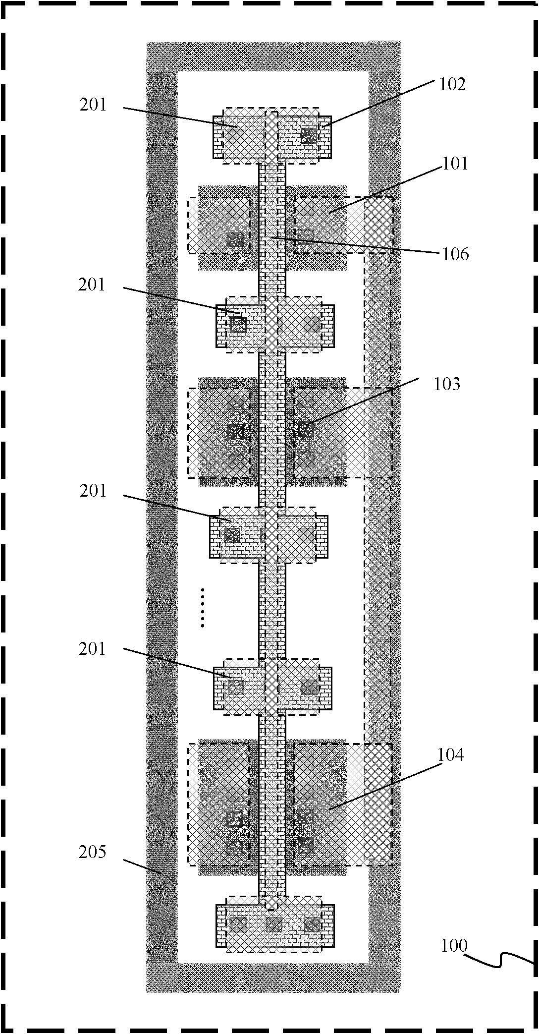
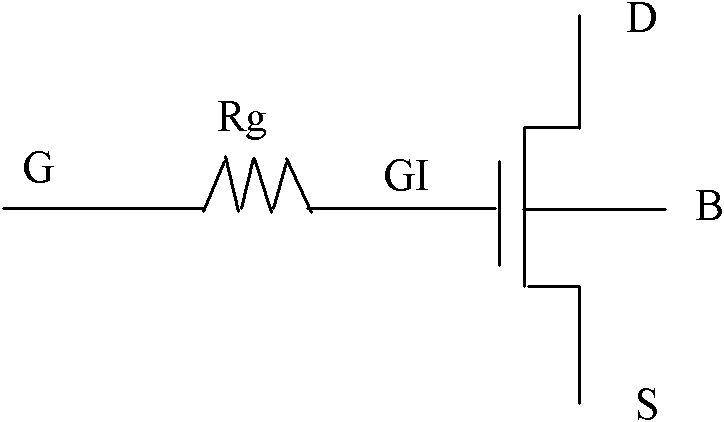
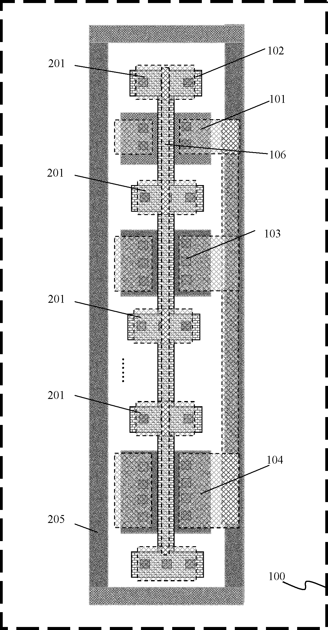
[0032] The MOS transistor gate resistance test structure of the present invention includes m groups of MOS transistors, each group of MOS transistors includes n MOS transistors with different channel widths, the same group of MOS transistors has the same channel length, and different groups of MOS transistors have different channel widths. The length of the track, the type of each MOS transistor is the same (both N-type or both P-type), m and n are positive integers;

[0033] The channel length L of the e-group MOS transistor e For: L e = L min +e*ΔL,L min is the minimum channel length, ΔL is the channel length difference, e is an integer greater than or equal to 0 and less than or equal to m-1, that is, the channel lengths of each group of MOS transistors are: L 0 = L min , L 1 = L min +ΔL, L 2 =Lmin+2ΔL,...,L m-1 = L min +(m-1)ΔL; the channel length of each group of MOS transistors is based on compliance with the design rules, and a short channel device is selected....


PUM

PropertyMeasurementUnit
Channel lengthaaaaaaaaaa
Channel widthaaaaaaaaaa

Abstract

The invention discloses a grid resistor test structure for a metal-oxide-semiconductor (MOS) transistor. The test structure includes m groups of MOS transistors; each group of the MOS transistors comprises n MOS transistors with various channel widths, wherein the MOS transistors in the same group have the identical channel length and different groups of MOS transistors have different channel lengths; and all the MOS transistors have the same type. According to the grid resistor test structure of MOS transistors, all coefficients in a resistance element Rg functional expression in an MOS transistor model can be visually obtained with consideration of the influence of a grid resistor on MOS transistor characteristics.

Description

technical field [0001] The invention relates to semiconductor test technology, in particular to a test structure for quantifying the influence of grid resistance on device characteristics. Background technique [0002] As the size of MOS (Metal-Oxide-Semiconductor, Metal-Oxide-Semiconductor) transistors shrinks, the influence of gate resistance on the characteristics of MOS transistors is gradually increasing, especially in 45nm and below processes. When establishing MOS transistor models, it is necessary to This factor is introduced. [0003] When considering the effect of the gate resistance on the characteristics of the MOS transistor, the model of the MOS transistor is as figure 2 As shown, a resistance element Rg is mainly added to the gate of the MOS transistor, and the resistance element Rg can be expressed as a function of the channel length L, channel width W, and temperature T of the MOS transistor: Rg=Func(W, L, T). [0004] However, based on the prior art, it ...

Claims


Application Information

Patent Timeline
IPC IPC(8): H01L23/544
Inventor 刘梅李平梁
Owner SHANGHAI HUAHONG GRACE SEMICON MFG CORP
Why Eureka
Try Eureka