Printed circuit board (PCB) layer-by-layer para-position laser drilling method

A laser, copper layer technology, applied in laser welding equipment, electrical components, printed circuit manufacturing, etc., can solve the difficulty of low inter-layer alignment, increased blind hole position offset, and increased blind hole to bottom PAD position accuracy and other problems to achieve the effect of solving the partial hole in the inner layer

Active Publication Date: 2012-10-03
GUANGZHOU MEADVILLE ELECTRONICS
View PDF2 Cites 32 Cited by
  • Summary
  • Abstract
  • Description
  • Claims
  • Application Information

AI Technical Summary

Problems solved by technology

[0005] (2) Due to the low inter-layer alignment of the alignment target pattern superposition, when the designed target pattern (L02/L03) is offset, such as Figure 1b As shown, due to the small design of the inner PAD, the blind hole (L0102/L0403) deviates from the inner PAD or even collapses (that is, the blind hole deviates from the bottom PAD)
[0006]

Method used


Image

  • Printed circuit board (PCB) layer-by-layer para-position laser drilling method
  • Printed circuit board (PCB) layer-by-layer para-position laser drilling method
  • Printed circuit board (PCB) layer-by-layer para-position laser drilling method

Examples


Embodiment Construction

[0023] In the following, the method for layer-by-layer alignment laser drilling of PCBs of the present invention will be further described in conjunction with the accompanying drawings and specific implementation methods, so as to understand the technical idea claimed by the present invention more clearly.

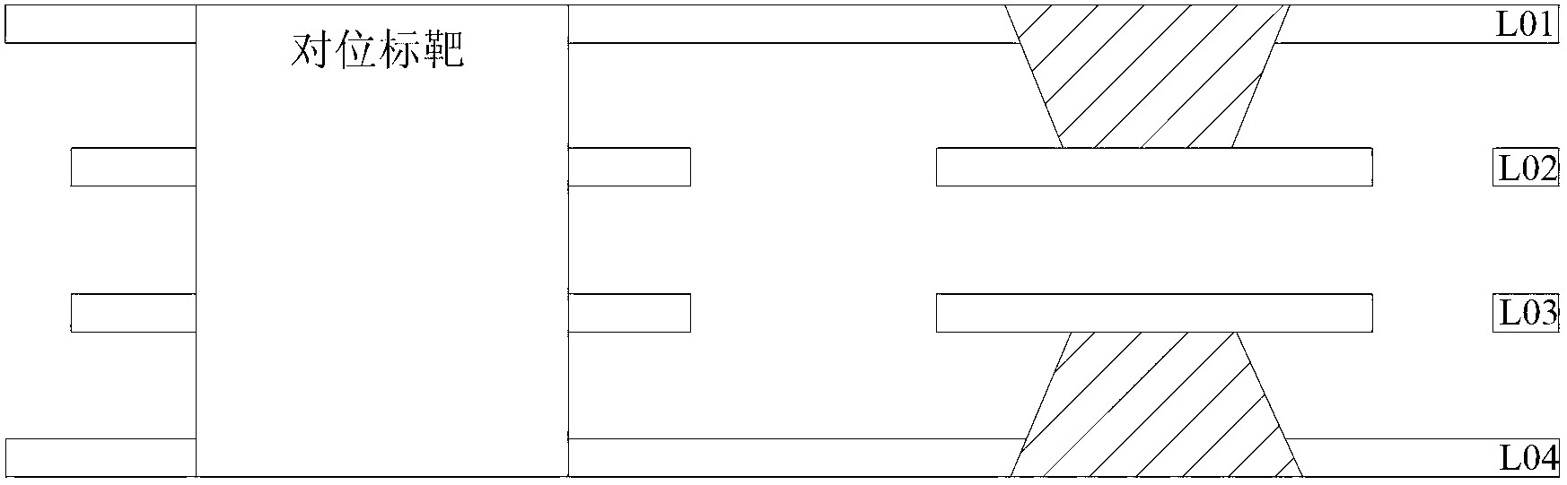
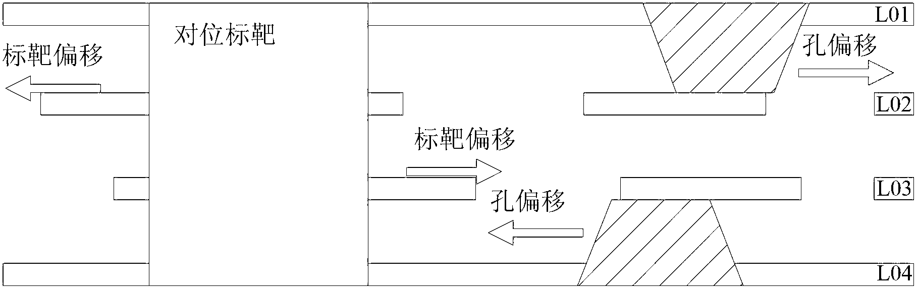
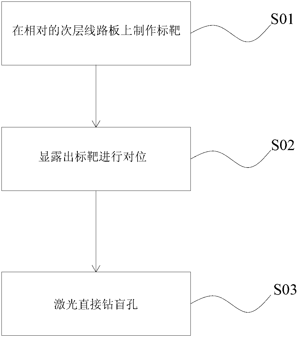
[0024] Such as figure 2 As shown, the method of layer-by-layer alignment laser drilling of PCB includes the following steps:

[0025] S01, making a target on the relative sub-layer circuit board;

[0026] The relative sub-layer circuit board here is relative to the sub-layer circuit board in the technical field. The sub-layer circuit board in the technical field refers to the inner layer of the outermost circuit board, which is called the sub-layer. For example, in In the eight-layer board, the second layer and the seventh layer are called the sub-layer, and in the present invention, the relative sub-layer circuit board refers to the inner layer of the circuit board of o...


PUM


Abstract

The invention relates to a printed circuit board (PCB) layer-by-layer para-position laser drilling method. The PCB layer-by-layer para-position laser drilling method comprises the following steps: manufacturing a target on the opposite second layer of circuit board; removing a copper layer covered on the target or removing a copper layer and a resin layer covered on the target, exposing the target and performing para-position; and directing drilling a blind hole by using laser. Owing to the PCB layer-by-layer para-position laser drilling method, the problem of hole misregistration of the blind hole on the inner layer can be effectively solved.

Description

[0001] technical field [0002] The invention relates to a manufacturing method of a printed circuit board, in particular to a method for layer-by-layer aligning laser drilling of blind holes in a PCB. Background technique [0003] At present, the production of printed circuit boards is developing in the direction of high precision and density. Due to the influence of circuit design, the design of PAD (pad) at the bottom of blind holes tends to be smaller. At the same time, due to the influence of offset between board layers, traditional X-RAY drilling targets are used. (Twice outer layers of graphics are superimposed), which is easy to cause blind holes to collapse. Taking a 4-layer circuit board as an example, [0004] (1) When the designed alignment target pattern (L02 / L03) has no offset, such as Figure 1a As shown, the blind hole (L0102 / L0403) has no or small offset to the inner PAD, where L02 / L03 refers to the design of the alignment target pattern on the L02 circuit b...

Claims


Application Information

Patent Timeline
IPC IPC(8): H05K3/00H05K3/40B23K26/36B23K26/386
Inventor 胡翠儿姚晓建
Owner GUANGZHOU MEADVILLE ELECTRONICS
Why Eureka
Try Eureka