Check patentability & draft patents in minutes with Patsnap Eureka AI!

A strained BiCMOS integrated device based on triple polycrystalline sige HBT and its preparation method

A technology for integrating devices and devices, which is applied in the field of strained BiCMOS integrated devices and preparations based on triple-polycrystalline SiGeHBT, and can solve problems such as lack of alternative silicon-based processes, restrictions on the development of Si integrated circuit manufacturing processes, and increased integration and complexity.

Inactive Publication Date: 2016-03-30
XIDIAN UNIV
View PDF2 Cites 0 Cited by
  • Summary
  • Abstract
  • Description
  • Claims
  • Application Information

AI Technical Summary

Problems solved by technology

[0003] SiCMOS integrated circuits have the advantages of low power consumption, high integration, low noise and high reliability, and occupy a dominant position in the semiconductor integrated circuit industry. However, with the further increase in the scale of integrated circuits, the reduction of device feature sizes, The increase in integration and complexity, especially after the feature size of the device enters the nanometer scale, the limitations of the material and physical characteristics of SiCMOS devices have gradually emerged, which limits the further development of Si integrated circuits and their manufacturing processes; although microelectronics Great progress has been made in the research and application of compound semiconductors and other new materials, but they are far from being able to replace silicon-based processes; and according to the development law of science and technology, a new technology has been It generally takes 20 to 30 years to become the main technology

Method used


Image

  • A strained BiCMOS integrated device based on triple polycrystalline sige HBT and its preparation method

Examples


Embodiment 1

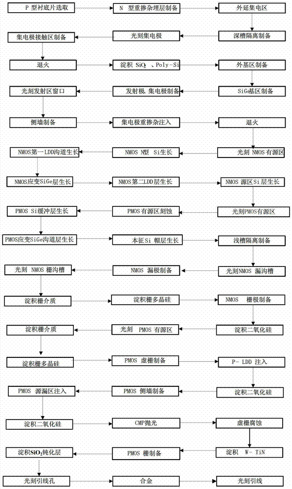
[0142] Embodiment 1: Prepare a strained BiCMOS integrated device and circuit based on a three-polycrystalline SiGeHBT with a conductive channel of 45nm, and the specific steps are as follows:

[0143] Step 1, epitaxial growth.

[0144] (1a) Select the doping concentration to be 5×10 14 cm -3 A P-type Si sheet as a substrate;

[0145] (1b) Thermally oxidize a layer of SiO with a thickness of 300nm on the substrate surface 2 layer;

[0146] (1c) Photoetching the buried layer region, implanting N-type impurities into the buried layer region, and annealing at 800° C. for 90 minutes to activate the impurities to form an N-type heavily doped buried layer region.

[0147] Step 2, isolation area preparation.

[0148] (2a) Remove the excess oxide layer on the surface, and epitaxially grow a layer with a doping concentration of 1×10 16 cm -3 The Si layer, with a thickness of 2 μm, serves as the collector area;

[0149] (2b) Thermally oxidize a layer of SiO with a thickness of 30...

Embodiment 2

[0225] Embodiment 2: The conductive channel is prepared as a strained BiCMOS integrated device and circuit based on three-polycrystalline SiGeHBT, and the specific steps are as follows:

[0226] Step 1, epitaxial growth.

[0227] (1a) Select the doping concentration as 1×10 15 cm -3 A P-type Si sheet as a substrate;

[0228] (1b) Thermally oxidize a layer of SiO with a thickness of 400nm on the substrate surface 2 layer;

[0229] (1c) Photoetching the buried layer region, implanting N-type impurities into the buried layer region, and annealing at 900° C. for 60 minutes to activate the impurities to form an N-type heavily doped buried layer region.

[0230] Step 2, isolation area preparation.

[0231] (2a) Remove the excess oxide layer on the surface, and epitaxially grow a layer with a doping concentration of 5×10 16 cm -3 A Si layer with a thickness of 2.5 μm acts as a collector area;

[0232] (2b) Thermally oxidize a layer of SiO with a thickness of 400nm on the surf...

Embodiment 3

[0307] Embodiment 3: Prepare a strained BiCMOS integrated device and circuit based on a three-polycrystalline SiGeHBT with a conductive channel of 22nm, and the specific steps are as follows:

[0308] Step 1, epitaxial growth.

[0309] (1a) Select the doping concentration to be 5×10 15 cm -3 A P-type Si sheet as a substrate;

[0310] (1b) Thermally oxidize a layer of SiO with a thickness of 500nm on the surface of the substrate 2 layer;

[0311] (1c) Photoetching the buried layer region, implanting N-type impurities into the buried layer region, and annealing at 950° C. for 30 minutes to activate the impurities to form an N-type heavily doped buried layer region.

[0312] Step 2, isolation area preparation.

[0313] (2a) Remove the excess oxide layer on the surface, and epitaxially grow a layer with a doping concentration of 1×10 17 cm -3 The Si layer, with a thickness of 3 μm, serves as the collector area;

[0314] (2b) Thermally oxidize a layer of SiO with a thicknes...


PUM

PropertyMeasurementUnit
thicknessaaaaaaaaaa
thicknessaaaaaaaaaa
thicknessaaaaaaaaaa

Abstract

The invention discloses a strain BiCMOS (Bipolar Complementary Metal-Oxide-Semiconductor Transistor) integrated device based on a tri-polycrystal SiGe HBT (Heterojunction Bipolar Transistor) and a preparation method thereof. The preparation method comprises the steps of: first, preparing the tri-polycrystal SiGe HBT on a Si substrate by a self-aligning process; then, respectively growing an N type Si epitaxial layer, an N type strain SiGe layer, a P type strain SiGe layer, an N type strain SiGe layer, and an N type Si layer as well as an N type Si layer, an N type strain SiGe layer, and an N type Si cap layer in active regions of an NMOS (N-channel Metal Oxide Semiconductor) device and a PMOS (P-channel Metal Oxide Semiconductor) device on the substrate to prepare a drain electrode, a grid electrode and a source region in the active region of the NMOS device so as to prepare the NMOS device; and preparing a virtual grid electrode in the active region of the PMOS device, depositing a dielectric layer to form a grid side wall, and injecting and forming a source electrode and a drain electrode of the PMOS device by the self-aligning process to form the grid electrode to prepare the PMOS device, so as to form the strain BiCMOS integrated device and a circuit, wherein the channel of an MOS (Metal Oxide Semiconductor) device is 22-45nm. According to the strain BiCMOS integrated device based on the tri-polycrystal SiGe HBT and the preparation method of the strain BiCMOS integrated device based on the tri-polycrystal SiGe HBT provided by the invention, a performance-enhanced strain BiCMOS integrated circuit based on the tri-polycrystal SiGe HBT is prepared in a low temperature process by means of the characteristic that the vertical electronic mobility and the horizontal hole mobility of the strain SiGe material are greater than those of relaxation Si adequately.

Description

technical field [0001] The invention belongs to the technical field of semiconductor integrated circuits, and in particular relates to a strained BiCMOS integrated device based on triple-polycrystalline SiGeHBT and a preparation method thereof. Background technique [0002] Semiconductor integrated circuits are the foundation of the electronics industry, and people's huge demand for the electronics industry has prompted the rapid development of this field. In the past few decades, the rapid development of the electronics industry has had a huge impact on social development and the national economy; at present, the electronics industry has become the largest industry in the world, occupying a large share in the global market, with output value Already over $1 trillion. [0003] SiCMOS integrated circuits have the advantages of low power consumption, high integration, low noise and high reliability, and occupy a dominant position in the semiconductor integrated circuit indust...

Claims


Application Information

Patent Timeline
Patent Type & Authority Patents(China)
IPC IPC(8): H01L27/06H01L21/8249
Inventor 宋建军胡辉勇李妤晨宣荣喜张鹤鸣舒斌戴显英郝跃
Owner XIDIAN UNIV
Features
  • R&D
  • Intellectual Property
  • Life Sciences
  • Materials
  • Tech Scout
  • Unparalleled Data Quality
  • Higher Quality Content
  • 60% Fewer Hallucinations
Learn More