Structure of package substrate and manufacturing method of package substrate

A technology for packaging substrates and manufacturing methods, which is applied in semiconductor/solid-state device manufacturing, electrical components, electric solid-state devices, etc., can solve problems such as the reliability of the contact joint surface of circuit substrates, and achieve signal transmission effects and electrical connections. Structurally Reliable Effects

Active Publication Date: 2013-01-30
ASE SHANGHAI
View PDF4 Cites 5 Cited by
  • Summary
  • Abstract
  • Description
  • Claims
  • Application Information

AI Technical Summary

Problems solved by technology

[0005] In view of this, the present invention provides a structure of a packaging substrate to solve the problem of the reliability of the contact joint surface of the circuit substrate existing in the prior art

Method used


Image

  • Structure of package substrate and manufacturing method of package substrate
  • Structure of package substrate and manufacturing method of package substrate
  • Structure of package substrate and manufacturing method of package substrate

Examples


Embodiment Construction

[0016] The following descriptions of the various embodiments refer to the accompanying drawings to illustrate specific embodiments in which the present invention can be practiced. Furthermore, the directional terms mentioned in the present invention, such as "upper", "lower", "top", "bottom", "front", "back", "left", "right", "inside", " Outer, Side, Surround, Center, Horizontal, Horizontal, Vertical, Longitudinal, Axial, Radial, Topmost, or Bottommost etc. are merely for reference to the directions of the attached drawings. Therefore, the directional terms used are used to illustrate and understand the present invention, but not to limit the present invention.

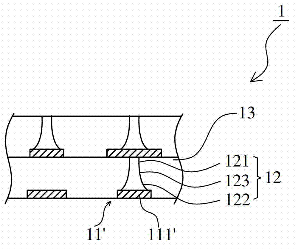
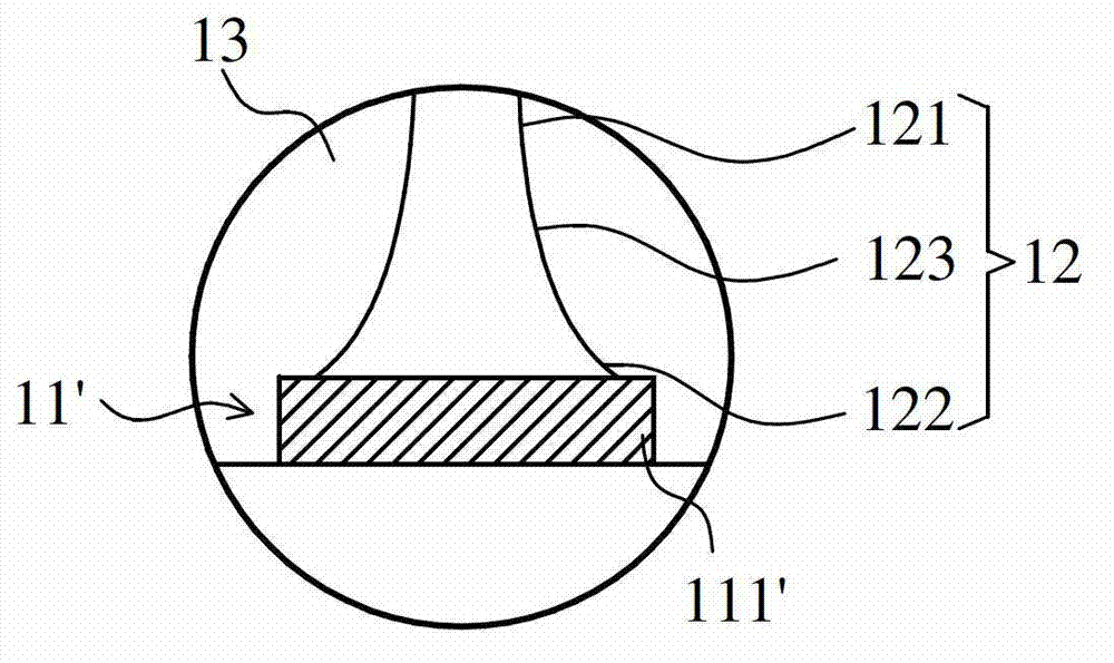
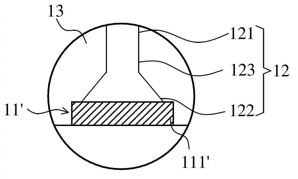
[0017] Please refer to figure 1 As shown, the packaging substrate 1 according to one embodiment of the present invention mainly includes: a circuit layer 11 ′, at least one connection pad 111 ′, at least one conductive column 12 and a dielectric layer 13 . The circuit layer 11' has at least one connection pad 111'....


PUM


Abstract

The invention discloses a structure of a package substrate and a manufacturing method of the package substrate. The package substrate comprises a circuit layer, at least one conductive column and a dielectric layer, wherein the circuit layer is provided with at least one connecting pad; the conductive columns are formed on the connecting pads; each conductive column is provided with a first surface, a second surface and a side wall connected with the first surface and the second surface; the area of each second surface is greater than that of the corresponding first surface; each second surface is combined to the corresponding connecting pad; and the dielectric layer covers the circuit layer and wraps the conductive columns.

Description

technical field [0001] The present invention relates to a structure of a packaging substrate and a manufacturing method thereof, in particular to a structure of a packaging substrate capable of increasing the bonding reliability of interlayer via holes and a manufacturing method thereof. Background technique [0002] Nowadays, in order to meet various high-density and miniaturized packaging requirements in the semiconductor packaging industry for more active and passive components and circuit loading, semiconductor packaging has gradually developed from double-layer circuits to multi-layer circuit boards (multi- layer circuit board), using interlayer connection technology (Interlayer connection) in a limited space to expand the available circuit layout area on the semiconductor packaging substrate (substrate), in order to meet the needs of integrated circuits with high circuit density and reduce the thickness of the packaging substrate , to accommodate a larger number of cir...

Claims


Application Information

Patent Timeline
Patent Type & Authority Applications(China)
IPC IPC(8): H01L23/14H01L21/48
Inventor 陆松涛黄建华王德峻罗光淋方仁广
Owner ASE SHANGHAI
Why Eureka
Try Eureka