

Non-buried layer double deep N well high-voltage isolation N-type LDMOS and method for manufacturing N-type LDMOS devices
A high-voltage isolation, N-type technology, used in semiconductor/solid-state device manufacturing, electrical components, circuits, etc., can solve problems such as cost increase, and achieve the effect of cost reduction, easy implementation, and performance improvement
- Summary
- Abstract
- Description
- Claims
- Application Information
AI Technical Summary
Problems solved by technology
Method used
Image

Examples
Embodiment Construction
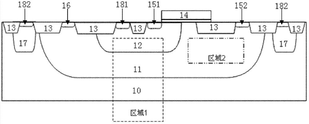
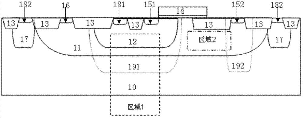
[0025] Such as figure 2 As shown, the double-deep N-type well high-voltage isolation N-type LDMOS device of the non-buried layer of the embodiment of the present invention includes: an N well 11 is provided on a P-type silicon substrate 10, and a P well 12 and a plurality of Isolation structure 13; above the N well 11 is a gate 14, one end of the gate 14 is located above the P well 12, and the other end is located above the isolation structure 13; there is an N-type heavily doped region 152 in the N well 11, and the N-type heavy The doped region 152 serves as the drain of the LDMOS device, the P well 12 has an N-type heavily doped region 151, and the N-type heavily doped region 151 serves as the source of the LDMOS device; there is a first deep N-type well below the P well 12 191, there is a second deep N-type well 192 under the N-type heavily doped region 152, and the depth and implantation concentration of the first deep N-type well 191 and the second deep N-type well 192 a...
PUM
 Abstract
Description
Claims
Application Information