Transverse variable doping terminal structure, design method and preparation method

A terminal structure and design method technology, applied in design optimization/simulation, semiconductor/solid-state device manufacturing, special data processing applications, etc., can solve problems such as low efficiency and difficulty in achieving optimal design, and achieve simple and uniform surface electric field distribution, the effect of improving the doping concentration distribution

Pending Publication Date: 2021-02-19
UNIV OF ELECTRONICS SCI & TECH OF CHINA
View PDF12 Cites 0 Cited by
  • Summary
  • Abstract
  • Description
  • Claims
  • Application Information

AI Technical Summary

Problems solved by technology

However, for the design of the VLD terminal structure, the simulation software is usually used to repeatedly simulate and iterate, the efficiency is low, and it is difficult to achieve the optimal design

Method used


Image

  • Transverse variable doping terminal structure, design method and preparation method
  • Transverse variable doping terminal structure, design method and preparation method
  • Transverse variable doping terminal structure, design method and preparation method

Examples


Embodiment 1

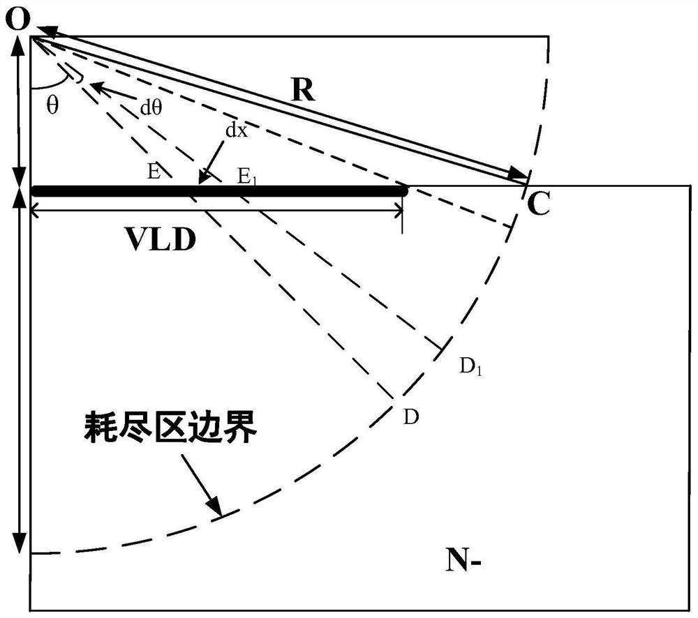
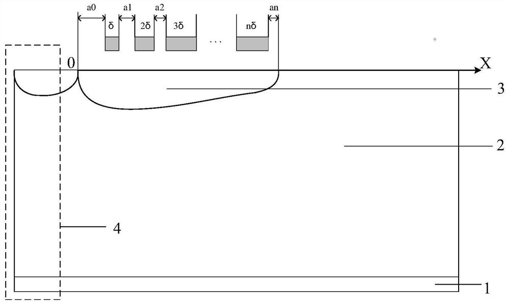
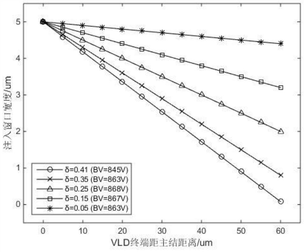
[0043] Design a lateral variable doping structure that meets the withstand voltage of 800V. Such as figure 2As shown, it includes a heavily doped first conductive type semiconductor substrate 1, a first conductive type semiconductor drift region 2 on the upper surface of the heavily doped first conductive type semiconductor substrate 1, and the first conductive type semiconductor drift region 2 The second conductivity type semiconductor terminal region 3 on the upper surface, the doping concentration of the first conductivity type semiconductor drift region 2 is N D , taking the starting position of the terminal region 3 of the second conductivity type near the active region 4 as the coordinate origin, and taking the upper surface of the semiconductor termination region 3 of the second conductivity type as the x-axis, so as to be close to the active region 4 of the device On the side of the region 4, pointing away from the active 4 side of the device is the positive directio...


PUM


Abstract

The invention belongs to the technical field of power semiconductor devices, and relates to optimization of a design method of a transverse variable doping terminal structure. According to the transverse variable doping terminal structure provided by the invention, the doping concentration distribution of the VLD terminal region is improved by optimizing the width of the mask window of the terminal region. According to the improved transverse variable doping terminal impurity concentration distribution, more uniform surface electric field distribution can be obtained, the device breakdown voltage is improved, implementation is easy, only the size of a mask window needs to be adjusted, and extra process steps are not needed.

Description

technical field [0001] The invention belongs to the technical field of power semiconductor devices, and relates to a lateral variable doping terminal structure, a design method, and a preparation method. Background technique [0002] A power semiconductor device is composed of a cell region and a terminal region. The design of the cell region affects parameters such as the threshold voltage, on-resistance, capacitance, and breakdown voltage of the device. The design of the terminal region mainly affects the breakdown voltage of the device. Field limiting rings and field plates are the most commonly used terminal structures. When the withstand voltage requirements of the device are high, the number of field limiting rings and field plates will increase accordingly, and as the number of field limiting rings increases, the withstand voltage of the terminal will decrease. It tends to be saturated, and the increase in the number of field limiting rings and field plates makes the ...

Claims


Application Information

Patent Timeline
Patent Type & Authority Applications(China)
IPC IPC(8): H01L29/06H01L21/266G06F30/20
CPCH01L29/0619H01L29/0684H01L21/266G06F30/20
Inventor 任敏蓝瑶瑶李吕强郭乔高巍李泽宏张波
Owner UNIV OF ELECTRONICS SCI & TECH OF CHINA
Why Eureka
Try Eureka