Manufacturing method of high voltage isolating N type laterally diffused metal oxide semiconductor (LDMOS) component

A manufacturing method, high-voltage isolation technology, applied in semiconductor/solid-state device manufacturing, semiconductor devices, electrical components, etc., can solve the problem of high cost

Active Publication Date: 2013-04-10
SHANGHAI HUAHONG GRACE SEMICON MFG CORP
View PDF3 Cites 10 Cited by
  • Summary
  • Abstract
  • Description
  • Claims
  • Application Information

AI Technical Summary

Problems solved by technology

[0012] In view of this situation, most of the prior art adopts the process method of N-type buried layer + epitaxy to meet the penetration requirements of PNP (P body-DNW-P type substrate) in the vertical direction of the device; The drain drift area is designed ...

Method used


Image

  • Manufacturing method of high voltage isolating N type laterally diffused metal oxide semiconductor (LDMOS) component
  • Manufacturing method of high voltage isolating N type laterally diffused metal oxide semiconductor (LDMOS) component
  • Manufacturing method of high voltage isolating N type laterally diffused metal oxide semiconductor (LDMOS) component

Examples


Embodiment Construction

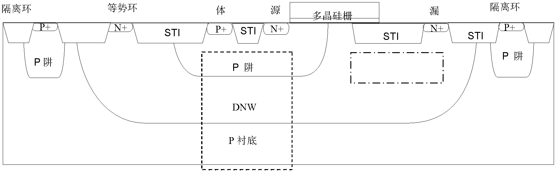
[0039] An embodiment of the manufacturing method of the high-voltage isolation N-type LDMOS device of the present invention is as follows Figure 2 to Figure 10 shown, including the following steps:

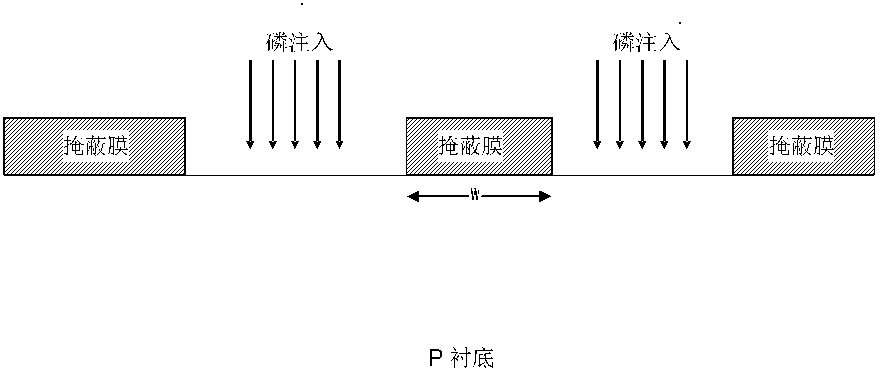
[0040] 1. Form a masking film on the P-type silicon substrate, etch the masking film to the upper surface of the silicon substrate, and form two very deep N-type wells on the left and right VDNW ion implantation selection windows, and the formed two very deep N-type wells on the left and right The width W of the masking film between the ion implantation selection windows is greater than 2um, such as figure 2 shown;

[0041] 2. Perform N-type ion implantation at the first concentration, such as 6E12 to 1E13 ions / CM 2 , Phosphorus ion implantation with an energy of 1000Kev~2000Kev, such as figure 2 shown;

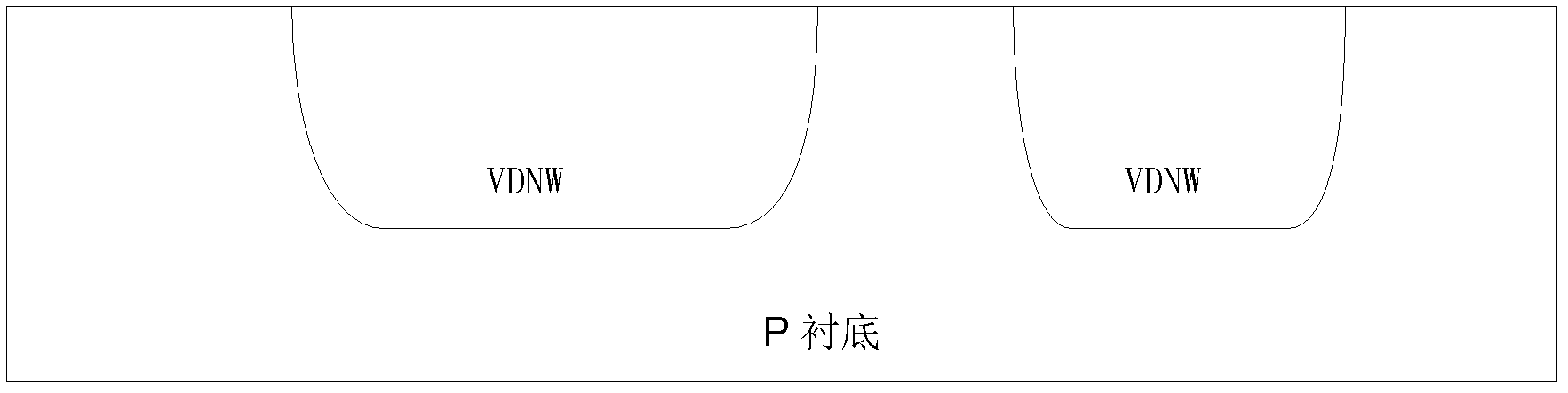
[0042] 3. Diffusion of N-type ions of the first intensity, such as phosphorus ion diffusion at a temperature of 1100°C to 1200°C for 5 to 10 hours, to form two very deep N...


PUM

PropertyMeasurementUnit
Widthaaaaaaaaaa
Widthaaaaaaaaaa

Abstract

The invention discloses a manufacturing method of a high voltage isolating N type laterally diffused metal oxide semiconductor (LDMOS) component. Firstly, relatively thick N type ions are respectively injected into the low portions of two different regions of the component, wherein the two different regions comprise a P type trap region and a leak end region. Two relatively deep isolated very deep N type traps are formed along with the strong deep push trap technology. Secondly, with the lighter injection condition, two relatively shallow communicated deep N type traps are formed along with the weak deep push trap condition, and then shallow junction depth is formed on a component leak end drift region. The manufacturing method of the high voltage isolating N type LDMOS component manufactures the high voltage isolating N type LDMOS component and has the advantages of being capable of guaranteeing withstand voltage of the component and optimization on resistance under a small lateral dimension and low in cost.

Description

technical field [0001] The invention relates to semiconductor technology, in particular to a manufacturing method of a high-voltage isolation N-type LDMOS device. Background technique [0002] High-voltage isolation N-type LDMOS (Lateral Double-diffused Metal-Oxide Semiconductor) devices are widely used in power management chip design due to their advantages of flexible design, low specific on-resistance (Rdson), and fast response speed. Compared with ordinary N-type LDMOS devices, high-voltage isolation N-type LDMOS devices will perform deep N-type well (Deep N well, DNW) implantation under the P-type well (P body) region for isolation purposes. Therefore, the potential connected to the source (source, N+) of the high-voltage isolated N-type LDMOS and the P-type well lead-out (bulk) can be connected at the potential (generally Vdd) of the zero potential (ground) and the drain (drain). , floating between the highest potential of the line). However, the source terminal (sou...

Claims


Application Information

Patent Timeline
IPC IPC(8): H01L21/336H01L21/266
CPCH01L29/0878H01L29/0886H01L29/66681H01L29/7816
Inventor 刘剑段文婷孙尧陈瑜陈华伦
Owner SHANGHAI HUAHONG GRACE SEMICON MFG CORP
Why Eureka
Try Eureka