High-voltage isolating N-type LDMOS device and manufacturing method thereof

A high-voltage isolation, N-type technology, applied in semiconductor/solid-state device manufacturing, semiconductor devices, electrical components, etc., can solve the problem of high cost, achieve performance improvement, easy implementation, simple and flexible process

Active Publication Date: 2013-07-03
SHANGHAI HUAHONG GRACE SEMICON MFG CORP
View PDF5 Cites 2 Cited by
  • Summary
  • Abstract
  • Description
  • Claims
  • Application Information

AI Technical Summary

Problems solved by technology

[0012] In view of this situation, most of the prior art adopts the process method of N-type buried layer + epitaxy to meet the penetration requirements of PNP (P body-DNW-P type substrate) in the vertical direction of the device; The drain drift area is designed using the Resurf method in order to optimize the withstand voltage and specific on-resistance (Rdson) of the device, thereby improving device performance. However, the process method of N-type buried layer + epitaxy is adopted, and The method of Resurf is more expensive

Method used


Image

  • High-voltage isolating N-type LDMOS device and manufacturing method thereof
  • High-voltage isolating N-type LDMOS device and manufacturing method thereof

Examples


Embodiment Construction

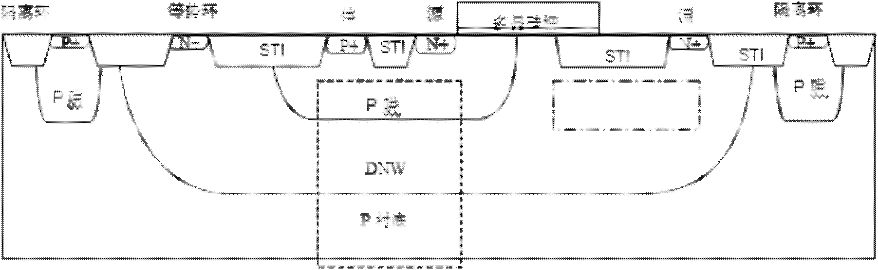
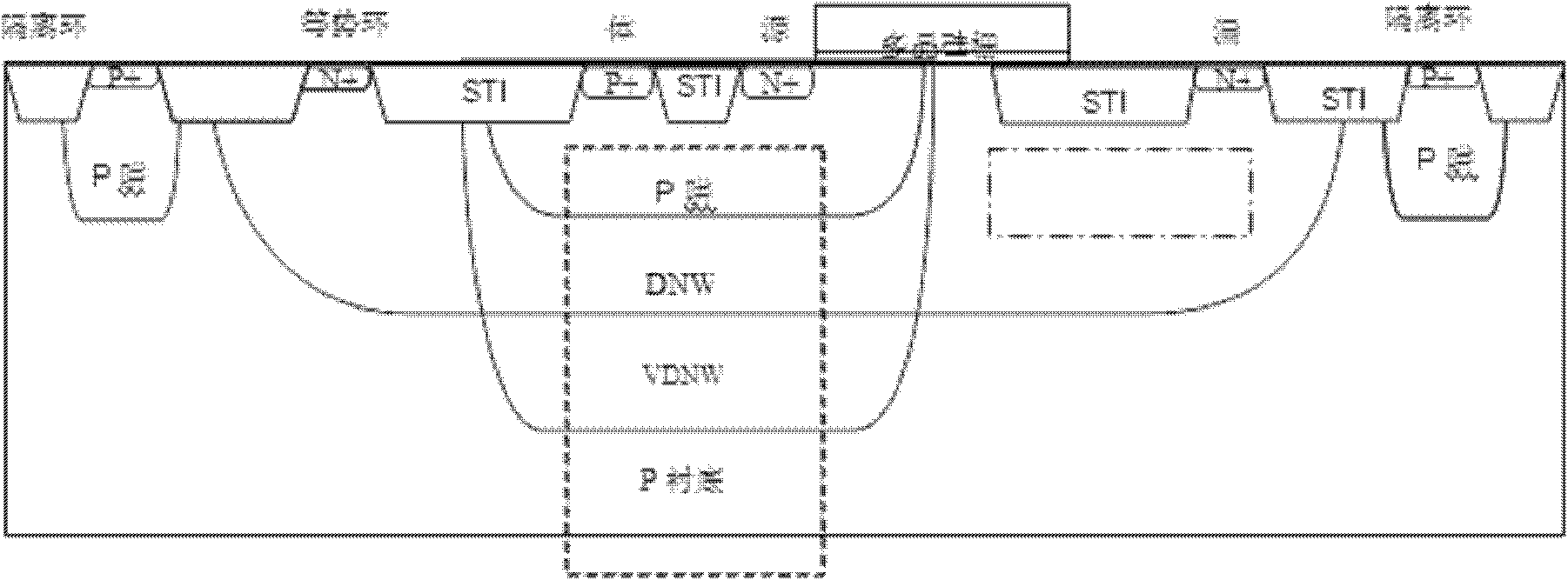
[0028] An embodiment of the high-voltage isolation N-type LDMOS device of the present invention is figure 2 As shown, a deep N-type well DNW is formed on the P-type substrate, and a very deep N-type well VDNW deeper than the deep N-type well DNW is formed in the deep N-type well DNW. A P-type well is formed in the N-type well VDNW, a polysilicon gate is formed above the adjacent region of the P-type well and the deep N-type well DNW, and a polysilicon gate is formed on the P-type well located on one side of the polysilicon gate. The source terminal and the body terminal are formed with a drain terminal on the deep N-type well on the opposite side of the polysilicon gate. figure 2 , the dotted line area is a PNP (P body-DNW-P type substrate) structure in the vertical direction, and the dotted line area is a drain terminal N-type drift region (drain drift).

[0029] Preferably, the depth of the deep N-type well is one-third to three-quarters of the depth of the very deep N-ty...


PUM


Abstract

The invention discloses a high-voltage isolating N-type LDMOS (Laterally Diffused Metal Oxide Semiconductor) device. A deep N well is formed on a P substrate; a very deep N well deeper than the deep N well is formed in the deep N well; a P body is formed in the very deep N well; a polysilicon gate is formed above an adjacent region between the P body and the deep N well; a device source and a device body are formed on the P body located on one side of the polysilicon gate; and a device drain is formed on the deep N well located on the opposite side of the polysilicon gate. The invention further discloses a manufacturing method of the high-voltage isolating N-type LDMOS device. The withstand voltage of the high-voltage isolating N-type LDMOS device can be ensured under a small lateral dimension, the specific on resistance is optimized, and the cost is low.

Description

technical field [0001] The invention relates to semiconductor technology, in particular to a high-voltage isolation N-type LDMOS device and a manufacturing method thereof. Background technique [0002] High-voltage isolation N-type LDMOS (Lateral Double-diffused Metal-Oxide Semiconductor) devices are widely used in power management chip design due to their advantages of flexible design, low specific on-resistance (Rdson), and fast response speed. Compared with ordinary N-type LDMOS devices, high-voltage isolation N-type LDMOS devices will perform deep N-type well (Deep N well, DNW) implantation under the P-type well (P body) region for isolation purposes. Therefore, the potential connected to the source (source, N+) of the high-voltage isolated N-type LDMOS and the P-type well lead-out (bulk) can be connected at the potential (generally Vdd) of the zero potential (ground) and the drain (drain). , floating between the highest potential of the line). However, the source term...

Claims


Application Information

Patent Timeline
Patent Type & Authority Applications(China)
IPC IPC(8): H01L29/06H01L29/78H01L21/336
Inventor 刘剑段文婷孙尧陈瑜陈华伦
Owner SHANGHAI HUAHONG GRACE SEMICON MFG CORP
Why Eureka
Try Eureka