Grooved gate MOS having buried layer structure

A technology of layer structure and groove gate, applied in the direction of electrical components, circuits, semiconductor devices, etc., can solve problems such as the increase of current flow path, the increase of device on-resistance, and the increase of channel resistance

Inactive Publication Date: 2016-09-28
UNIV OF ELECTRONICS SCI & TECH OF CHINA
View PDF4 Cites 8 Cited by
  • Summary
  • Abstract
  • Description
  • Claims
  • Application Information

AI Technical Summary

Problems solved by technology

However, when the device is turned on, the current flow path in part of the channel region increases, mak

Method used


Image

  • Grooved gate MOS having buried layer structure
  • Grooved gate MOS having buried layer structure
  • Grooved gate MOS having buried layer structure

Examples


Embodiment Construction

[0019] The present invention is described in detail below in conjunction with accompanying drawing

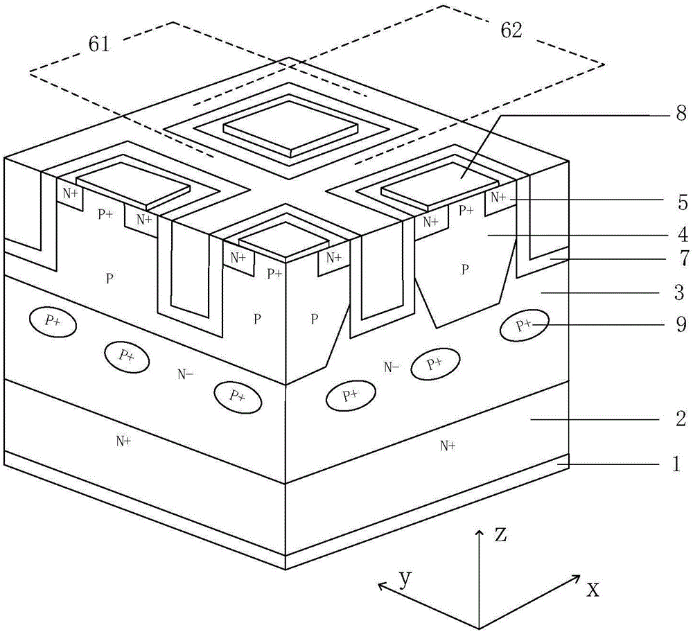
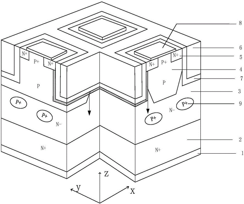
[0020] It should be noted that, like the coordinate axes in the drawings, the description corresponding to the coordinate axes in the present invention is that the lateral direction of the device corresponds to the x-axis direction, the longitudinal direction of the device corresponds to the y-direction, and the vertical direction of the device corresponds to the z-direction.

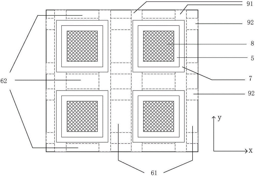
[0021] like figure 1 As shown, a trench gate MOS with a buried layer structure of the present invention includes a drain electrode 1, an N-type heavily doped single crystal silicon substrate 2 and an N- epitaxial layer 3 that are stacked sequentially from bottom to top; The upper layer of the N- epitaxial layer 3 has a first grooved gate structure 61, a second grooved gate structure 62 and a P-type body region 4; along the lateral direction of the device, both sides of the P-type body region 4 are the fi...


PUM


Abstract

The invention belongs to the technical field of power semiconductors, and in particular relates to a grooved gate MOS having a buried layer structure. Compared with conventional grooved gate MOSes, the grooved gate MOS herein introduces a P type body region having different depths in the x direction and y direction of a sketch map, such that the grooved gate is still provided with a P type region therebelow, which reduces the ratio between a grid leak capacitor (Cgd) and a grid source capacitor (Cgs) of the structure. An inverted-trapezoid P type body region in the x direction also improves peak electric field of a grooved gate corner region. A transverse electric field is introduced through the adding of a proper inverted buried layer area to an epitaxial layer area, which effectively increases pressure resistance capability of the grooved gate MOS. The added buried layer structure enables the N-epitaxial layer area below the grooved gate to be able to increase doped concentration and reduce on resistance.

Description

technical field [0001] The invention belongs to the technical field of power semiconductors, in particular to a trench gate MOS with a buried layer structure. Background technique [0002] Power VDMOS devices can generally be classified into planar gate VDMOS devices and trench gate VDMOS devices. Among them, the gate of the groove-gate VDMOS device is located in the silicon wafer. After the inversion layer channel is formed, a low-resistance channel is provided for the carriers. After entering the drift region, the current spreads across the entire cross-section of the cell. Without the JFET area, trench-gate VDMOS has a smaller on-resistance than planar-gate VDMOS. However, compared with the planar gate VDMOS, the trench gate VDMOS has poorer reliability. The main reason is that when the power trench gate VDMOS is switched under an inductive load, there will be electric field spikes at the sharp corners of the trench gate structure, resulting in failure. [0003] At pre...

Claims


Application Information

Patent Timeline
IPC IPC(8): H01L29/78H01L29/06
CPCH01L29/7813H01L29/0623H01L29/0684
Inventor 李泽宏陈哲曹晓峰李爽陈文梅任敏
Owner UNIV OF ELECTRONICS SCI & TECH OF CHINA
Why Eureka
Try Eureka