Un-assisted, low-trigger and high-holding voltage SCR

a low-trigger, high-holding voltage technology, applied in the field of scrs, can solve problems such as known problems that continue to exist in the prior art circui

Active Publication Date: 2010-05-18
SEMICON COMPONENTS IND LLC
View PDF5 Cites 26 Cited by
  • Summary
  • Abstract
  • Description
  • Claims
  • Application Information

AI Technical Summary

Benefits of technology

[0015]Illustratively, the particular device structure and processing steps of embodiments of the present invention provide the lower voltage triggering and the higher holding voltages without involving any external circuitry and without sacrificing the ESD protection robustness when compared to prior art devices. An embodiment of the present invention provides a protective SCR having an anode and a cathode built on an N-Well and an adjoining P-Well. Both of these Wells formed above an N-type epitaxial layer built onto a p-type substrate. An ESD structure is formed bridging the N-Well and the P-Well, where the ESD structure has a higher n-type doping density than the N-Well. A PLDD structure is formed in the P-Well at a lateral distance, L1, from the ESD structure. The PLDD structure has a doping level higher than the P-Well. An N+ structure, with a length of D5, is formed in the ESD structure, and the N+ structure has a higher n-type doping density than the ESD structure. A P+ structure, with a length of L, is formed in the PLDD structure, and the P+ structure has a higher p-type doping density than the PLDD structure. The edge of the N+ structure is located at a lateral distance LX from the nearest edge of the P+ structure, where the difference between L1 and LX determines, in part, the trigger voltage and the holding voltage of the protective SCR.

Problems solved by technology

Known problems continue to exist in the prior art circuit.

Method used


Image

  • Un-assisted, low-trigger and high-holding voltage SCR
  • Un-assisted, low-trigger and high-holding voltage SCR
  • Un-assisted, low-trigger and high-holding voltage SCR

Examples


Embodiment Construction

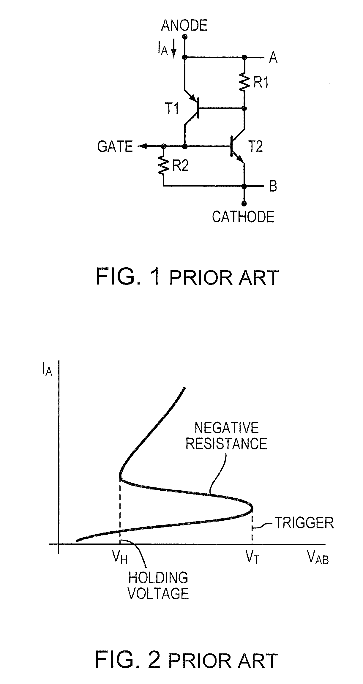
[0031]The above drawings and the text herein disclose a two terminal structure (no external trigger) for an SCR-type circuit with a trigger voltage as low as 8V. Moreover, the holding voltage may be tunable from about 5V to about 7.5V, while maintaining the trigger voltage essentially constant. That is, the holding voltage may be set from +5V to +7.5 volts while the trigger voltage remains at about +8V.

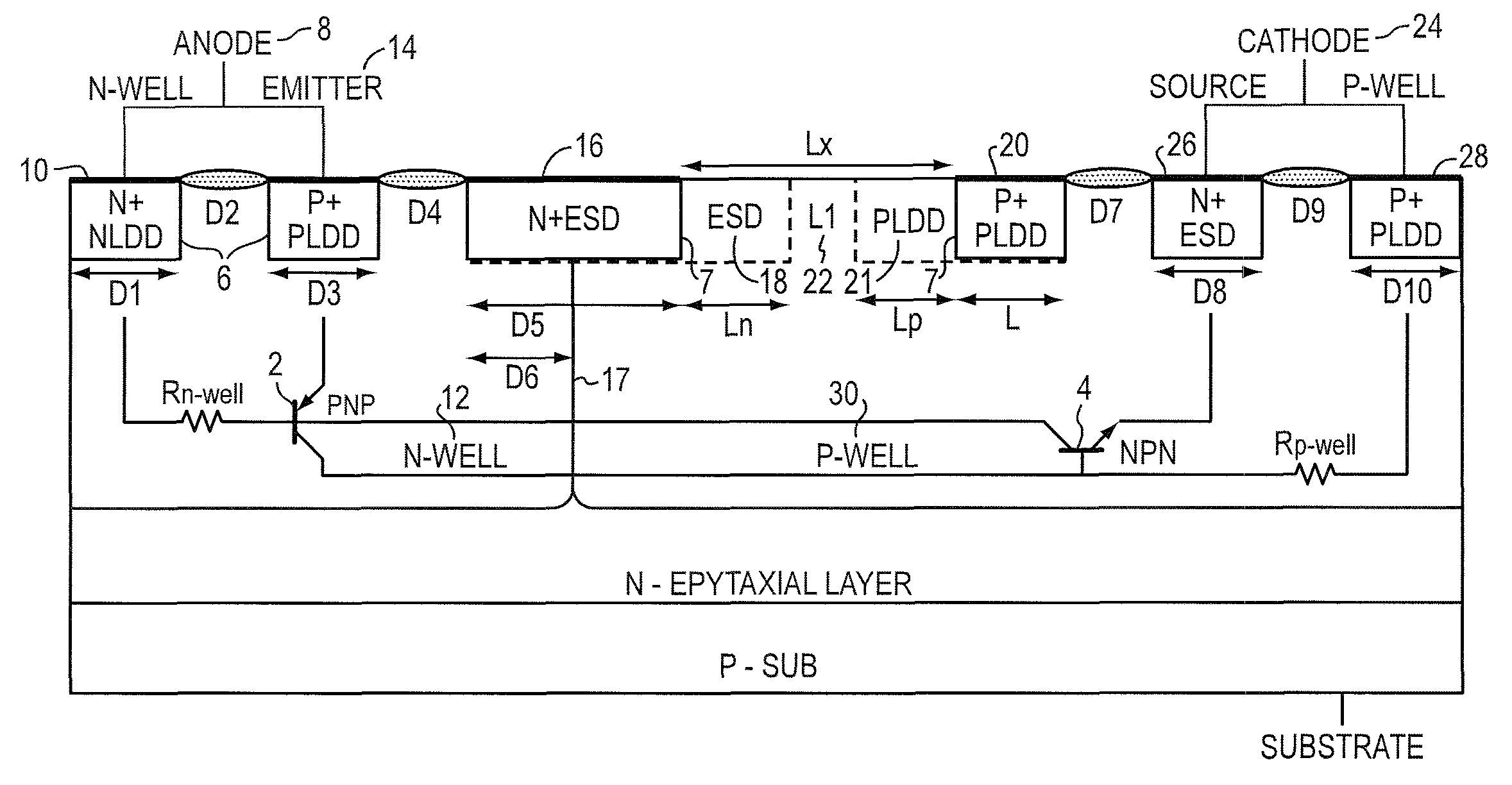
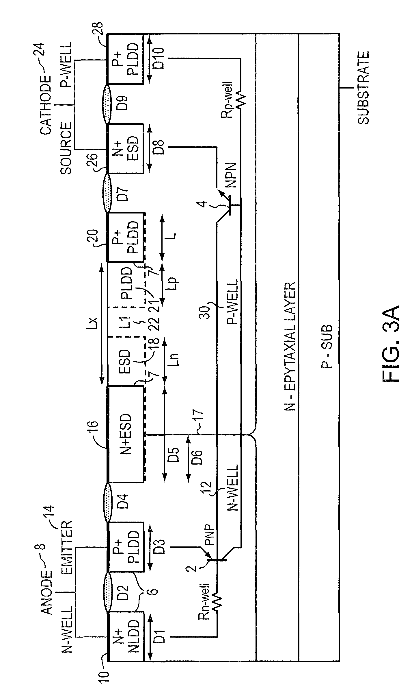
[0032]In FIG. 3A, a cross section of a protective device represents the bipolar PNP 2 and NPN 4 transistors approximately where they exist. Although the arrangement of the PNP 2 and the NPN 4 in FIG. 3A is similar to the schematic in FIG. 1, the differences in structure, dimensions and relative doping levels provide different advantageous characteristics. In the following descriptions, the dimensions, doping levels and materials used, the relative locations of the elements, and the resulting parameters and characteristics are illustrative. Those skilled in the art will be able to make...


PUM


Abstract

A protective SCR integrated circuit device is disclosed built on adjacent N and P wells and defining an anode and a cathode. In addition to the anode and cathode contact structures, the device has an n-type stack (N+ / ESD) structure bridging the N-Well and the P-Well, and a p-type stack (P+ / PLDD) structure in the P-Well. The separation of the n-type stack structure and the p-type stack structure provides a low triggering voltage without involving any external circuitry or terminal, that together with other physical dimensions and processing parameters also provide a relatively high holding voltage without sacrificing the ESD protection robustness. In an embodiment, the triggering voltage may be about 8V while exhibiting a holding voltage, that may be controlled by the lateral dimension of the n-type stack of about 5-7 V.

Description

CROSS REFERENCE TO RELATED APPLICATIONS[0001]The present application is related and claims the benefit of priority from the provisional application, Ser. No. 60 / 911,133, filed on Apr. 11, 2007, and of the same title, ownership and inventorship as the present application. The above referenced provisional application is hereby incorporated herein by reference.BACKGROUND OF THE INVENTION[0002]1. Field of the Invention[0003]The present invention relates silicon controlled rectifiers, SCRs, and more particularly to SCRs with controlled triggering and holding voltages.[0004]2. Background Information[0005]Protecting circuits from electrostatic discharges, where the protection is on the chip is an essential component for integrated circuits, especially newer, faster, smaller designs often found in very large scale integration, VLSI, circuits.[0006]FIG. 1 illustrates a traditional bipolar SCR protection device. This device may be fabricated using standard MOS processes (hence the “gate” term...

Claims


Application Information

Patent Timeline
Patent Type & Authority Patents(United States)
IPC IPC(8): H01L29/74
CPCH01L29/87H01L27/0262H01L23/60H01L27/04
Inventor LOU, LIFANGCHAPIN, JAY R.ROBINSON-HAHN, DONNA
Owner SEMICON COMPONENTS IND LLC
Why Eureka
Try Eureka