Layer for thin film photovoltaics and a solar cell made therefrom

a solar cell and thin film technology, applied in the field of photovoltaics, can solve the problems of inefficient use of available solar energy to produce electricity, and high cost of conventional solar cells, and achieve the effect of reducing the cost of conventional solar cells

Inactive Publication Date: 2010-09-30
FIRST SOLAR INC (US)
View PDF4 Cites 25 Cited by
  • Summary
  • Abstract
  • Description
  • Claims
  • Application Information

AI Technical Summary

Benefits of technology

[0004]In one embodiment, a photovoltaic device is provided. The device comprises a layer. The layer comprises a plurality of grains separated by grain boundaries wherein the grains are either p-type or n-type. The grain boundaries comprise an active dopant. The active dopant concentration in the grain boundaries is higher than the effective dopant concentration in the grains.

Problems solved by technology

Unfortunately, the available solar energy is not generally used efficiently to produce electricity.
The cost of conventional solar cells, and electricity generated by these cells, is generally very high.
Moreover, solar cells typically include multiple layers formed on a substrate, and thus solar cell manufacturing typically requires a significant number of processing steps.
As a result, the high number of processing steps, layers, interfaces, and complexity increase the amount of time and money required to manufacture these solar cells.

Method used


Image

  • Layer for thin film photovoltaics and a solar cell made therefrom
  • Layer for thin film photovoltaics and a solar cell made therefrom
  • Layer for thin film photovoltaics and a solar cell made therefrom

Examples


Embodiment Construction

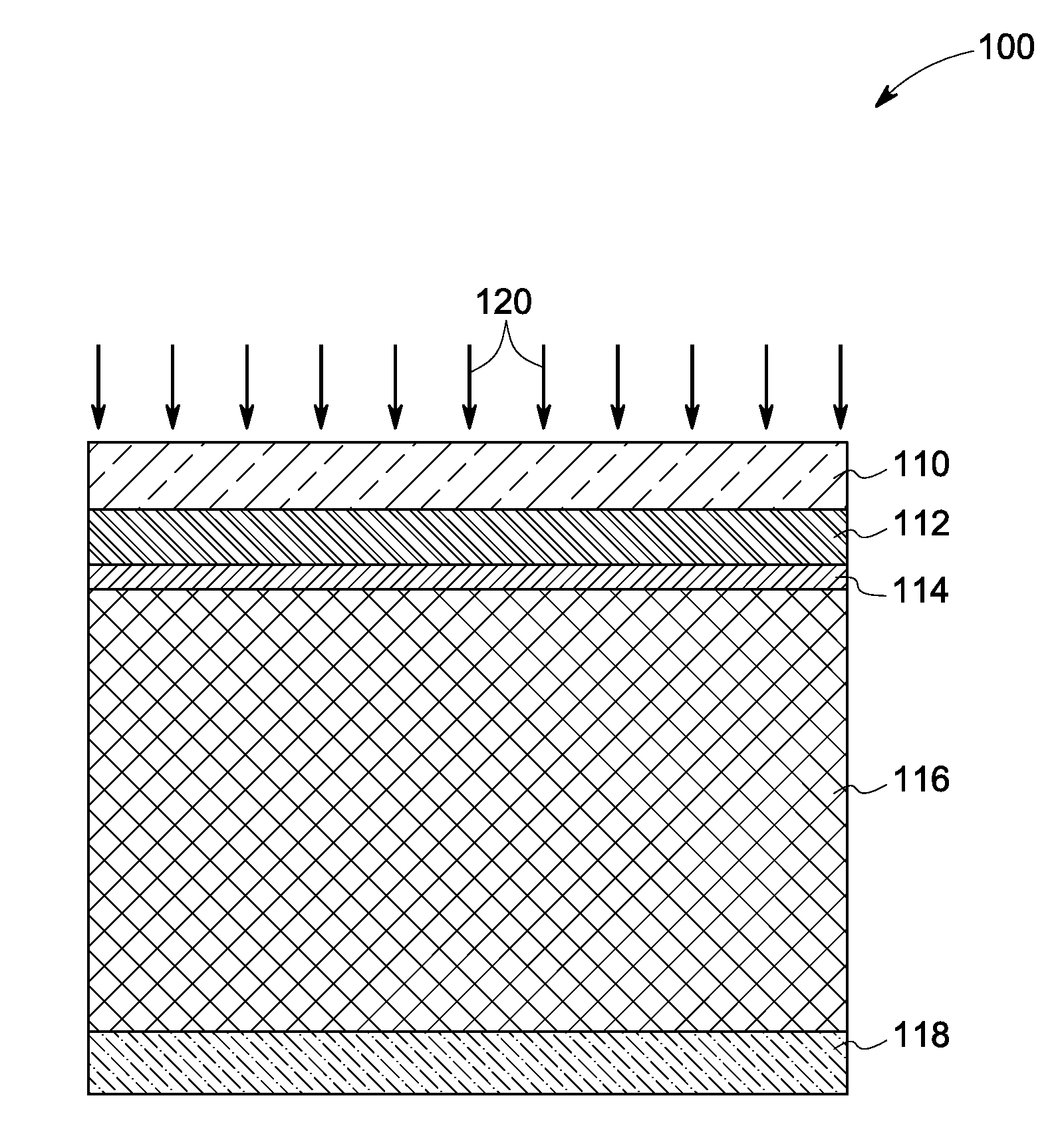
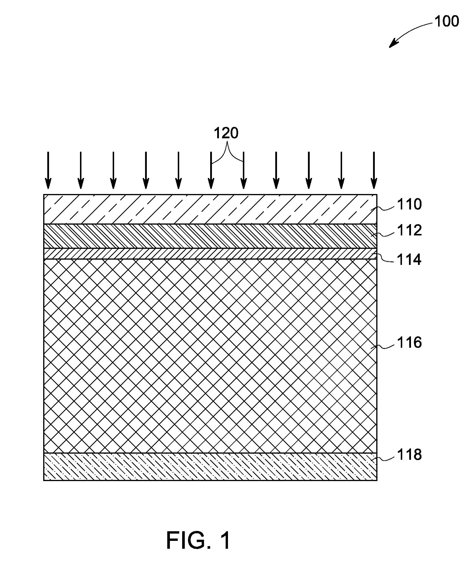
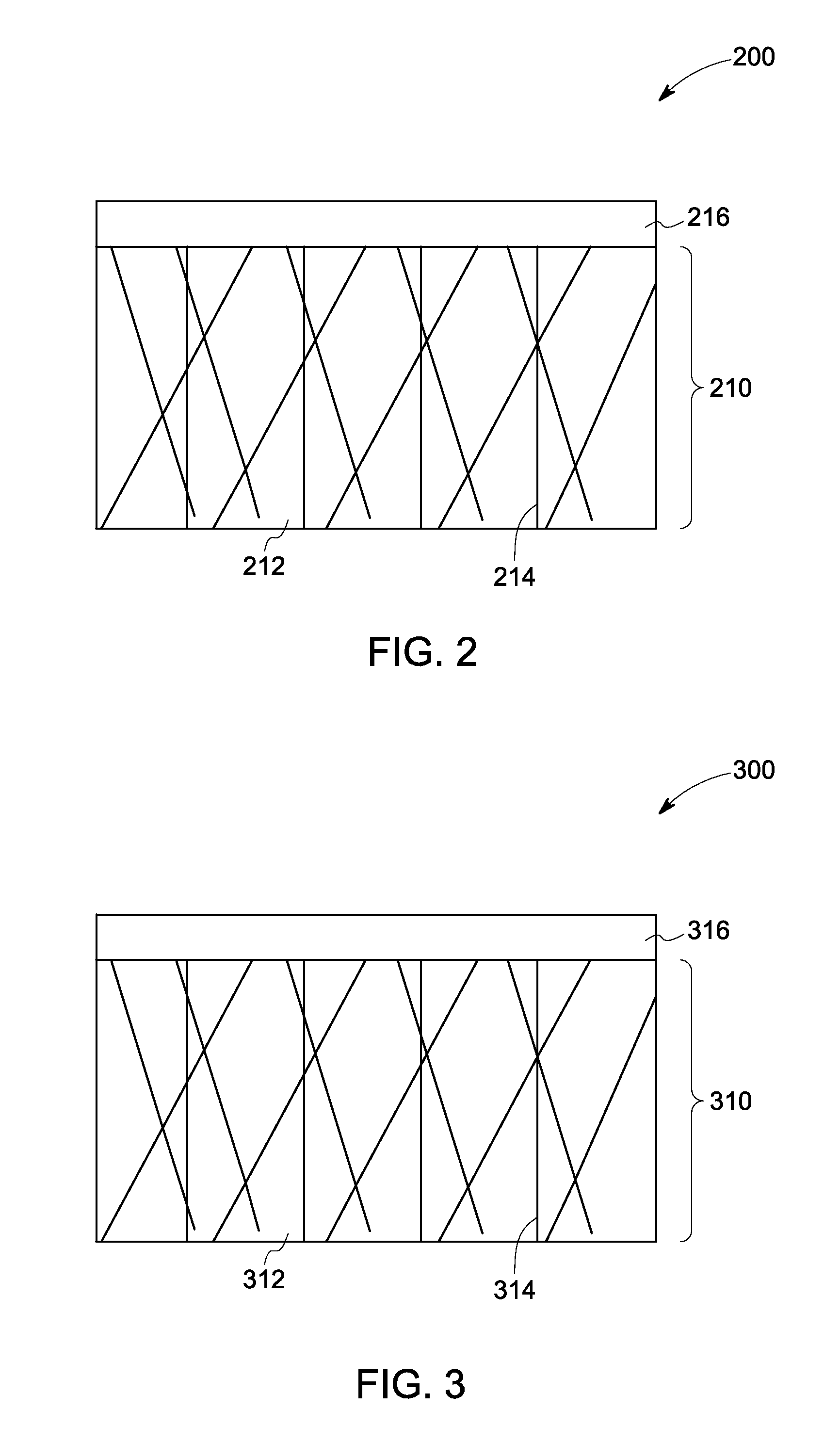
[0018]Cadmium telluride (CdTe) based solar devices known in the art typically demonstrate relatively low power conversion efficiencies, which may be attributed to a relatively low open circuit voltage (VOC) in relation to the bandgap of the material. This is due to the fact that the effective carrier concentration in CdTe is too low. Traditionally, the performance of a CdTe-based device has been explained by assigning bulk properties to the CdTe. However, there are increasing indications that the device performance is primarily controlled by the properties of the grain boundaries, and thus bulk properties only present an effective collective value of the whole film forming the solar cell.

[0019]Embodiments of the invention described herein address the noted shortcomings of the state of the art. The device described herein fills the needs described above by employing a doping method that will permit the addition of active dopants to the grain boundaries that will result in a layer wit...


PUM

PropertyMeasurementUnit
grain boundariesaaaaaaaaaa
concentrationaaaaaaaaaa
transparentaaaaaaaaaa

Abstract

A photovoltaic device is provided comprising a layer. The layer comprises a plurality of grains separated by grain boundaries wherein the grains are either p-type or n-type. The grain boundaries comprise an active dopant. The active dopant concentration in the grain boundaries is higher than the effective dopant concentration in the grains. The grains and grain boundaries may be of the same type or of the opposite type. Further, when the grain boundaries are n-type the bottom of the grain boundaries may be p-type. A method of making the layer is also disclosed.

Description

BACKGROUND[0001]The invention relates generally to the field of photovoltaics. In particular, the invention relates to a layer used in solar cells and a solar cell made therefrom.[0002]Solar energy is abundant in many parts of the world year around. Unfortunately, the available solar energy is not generally used efficiently to produce electricity. The cost of conventional solar cells, and electricity generated by these cells, is generally very high. For example, a typical solar cell achieves a conversion efficiency of less than 20 percent. Moreover, solar cells typically include multiple layers formed on a substrate, and thus solar cell manufacturing typically requires a significant number of processing steps. As a result, the high number of processing steps, layers, interfaces, and complexity increase the amount of time and money required to manufacture these solar cells.[0003]Accordingly, there remains a need for an improved solution to the long-standing problem of inefficient and...

Claims


Application Information

Patent Timeline
Patent Type & Authority Applications(United States)
IPC IPC(8): H01L31/00H01L31/036
CPCH01L31/02963H01L31/035281H01L31/03529Y02E10/543H01L31/1828H01L31/1836H01L31/073
Inventor KOREVAAR, BASTIAAN ARIEAHMAD, FAISAL RAZI
Owner FIRST SOLAR INC (US)
Why Eureka
Try Eureka