Method of and system for forming SiC crystals having spatially uniform doping impurities

a technology of doping impurities and crystals, applied in the direction of crystal growth process, crystal growth process, polycrystalline material growth, etc., can solve the problems of reducing the yield of high electronic quality substrates, difficult to achieve uniform electrical properties in other types of sic crystals, so as to achieve low yield and avoid generation. , the effect of low dopant concentration

Active Publication Date: 2009-10-27
II VI DELAWARE INC
View PDF13 Cites 28 Cited by
  • Summary
  • Abstract
  • Description
  • Claims
  • Application Information

AI Technical Summary

Benefits of technology

[0015]The present invention is a method for producing a spatially uniform and controlled concentration of a dopant throughout a SiC crystal boule. The method avoids or eliminates the too high dopant concentration in the first-to-grow boule portions and the too low dopant concentration in the last-to-grow portions. In accordance with the present invention, the dopant concentration can be sufficiently high to achieve the desired electronic properties of the SiC material while, at the same time, the dopant concentration can be low enough to avoid generation of crystal defects. In the doping method in accordance with the present invention, the dopant concentration does not change as the crystal grows. Therefore, longer boules with spatially uniform electrical properties can be grown resulting in higher quality of the SiC substrates, higher yields and productivity.

Problems solved by technology

Those skilled in the art of semiconductor materials know that production of SiC substrates with desirable electronic properties is impossible without purposeful introduction of certain impurities in a process known as doping.
With the exception of the nitrogen-doped crystals, attaining uniform electrical properties in other types of SiC crystals, including semi-insulating, p-type and phosphorus doped n-type crystals, is much more difficult because the doping compounds are not gaseous but solid.
For this reason, electrical properties of SiC crystals grown using the doping technique of prior art are spatially nonuniform and the yield of high electronic quality substrates is low.
Similar problems exist in the cases when other solid dopants are added to the SiC source 1 directly, including, but not limited to aluminum, boron and phosphorus.

Method used


Image

  • Method of and system for forming SiC crystals having spatially uniform doping impurities
  • Method of and system for forming SiC crystals having spatially uniform doping impurities
  • Method of and system for forming SiC crystals having spatially uniform doping impurities

Examples


example 1

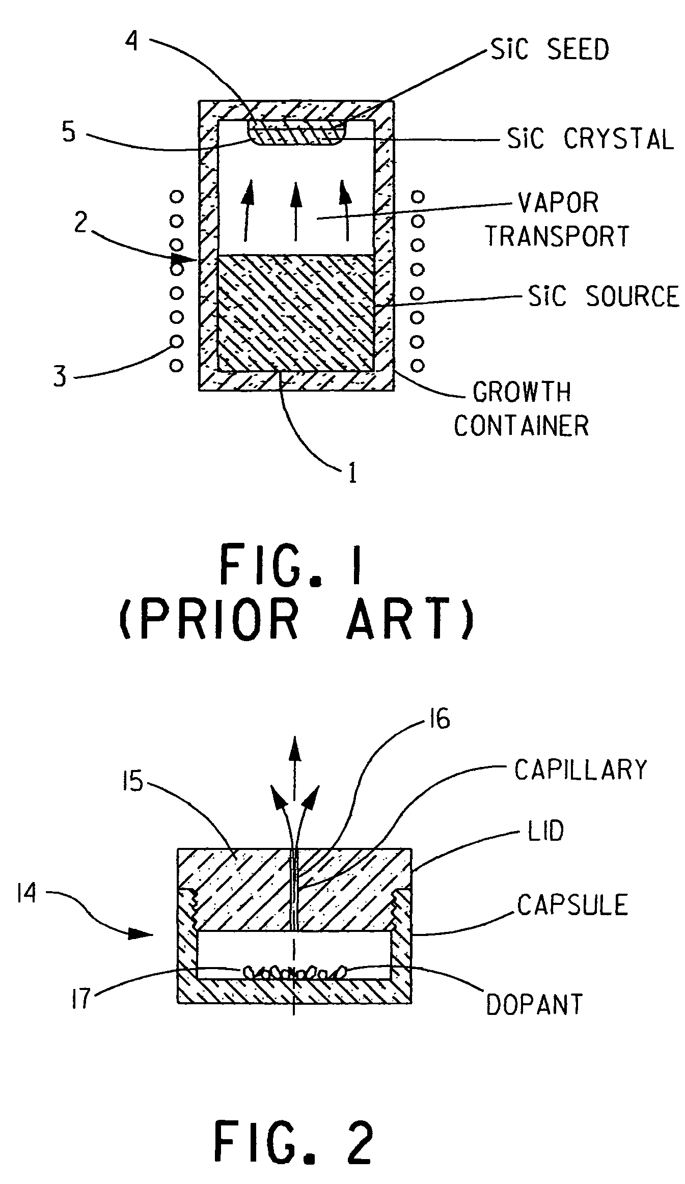
[0038]In accordance with the prior art SiC crystal growth method, an appropriate amount of elemental vanadium was admixed to the SiC source 1. The SiC source / vanadium mixture and a SiC seed 4 were loaded into growth container 2 which was then evacuated and filled with an inert gas to a desired pressure. Following this, the temperature of growth container 2 was raised to a temperature sufficient to cause the growth of the SiC crystal 5.

[0039]Thereafter, the grown SiC crystal 5 boule was sliced into wafers and the impurity content for vanadium and other elements was measured using Secondary Ion Mass Spectroscopy (SIMS) in wafer #2 and wafer #17 (the last wafer in the boule). The results showed that wafer #2 contained vanadium at about 1.4×1017 cm−3 while wafer #17 contained vanadium at about 2×1014 cm−3.

[0040]With reference to FIG. 4, the resistivity of each wafer obtained from the grown boule was measured and plotted. In the plot, each point represents an average resistivity for the ...

example 2

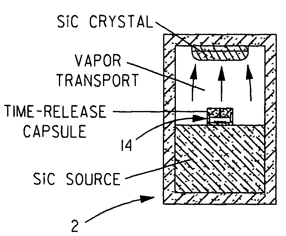
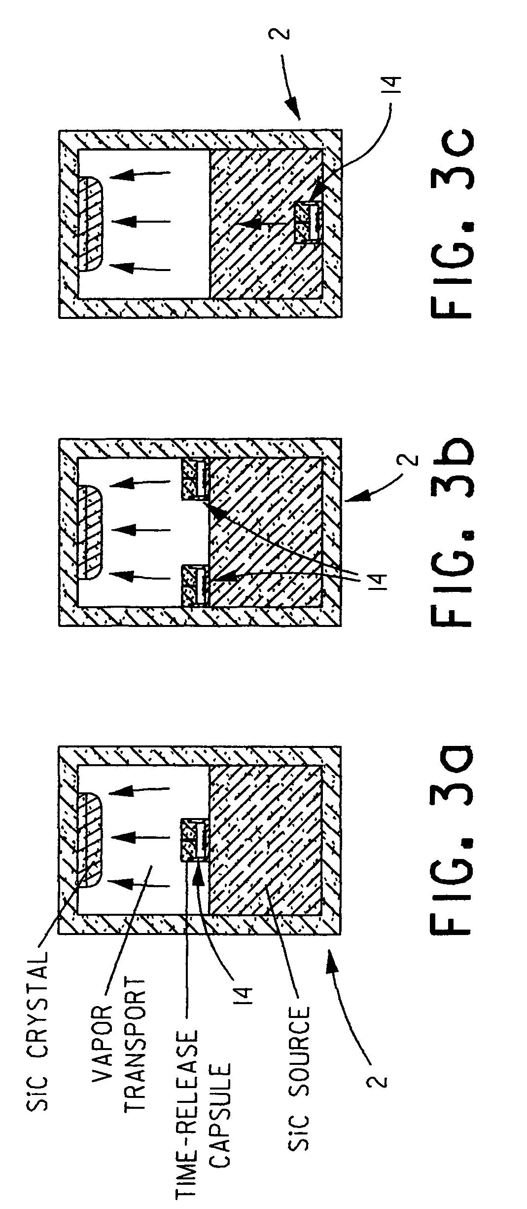
[0043]In accordance with a SiC crystal growth method of the present invention, a capsule 14 having a capillary 16 of 1.5 mm in diameter and 6 mm long was loaded with 1 g of pure vanadium carbide (VC0.88, 99.999+%). Capsule 14 was positioned atop the SiC source 1 in growth container 2. All other parameters of this growth run were in accordance with existing standard technological procedures.

[0044]After finishing this growth run and cooling to room temperature, capsule 14 was recovered and its content investigated. A pellet of sintered vanadium carbide was found inside capsule 14. Chemical analysis of the pellet showed that it consisted of vanadium and carbon in the stoichiometric ratio of VCx (x≈0.8) with traces of silicon accounting for less than 3 weight %. Thus, there was no major chemical transformation in capsule 14 during growth, and vanadium was preserved in its stable form of vanadium carbide. The traces of silicon could be a result of silicon diffusion through the capsule wa...

example 3

[0047]In accordance with a SiC crystal growth method of the present invention, a capsule 14 having a capillary 16 of 1.5 mm in diameter and 6 mm long was loaded with 1 g of elemental vanadium of 99.995% purity. Capsule 14 was positioned atop the SiC source 1 in growth container 2. All other parameters of this growth run were in accordance with existing standard technological procedures.

[0048]After finishing this growth run and cooling to room temperature, the capsule content was investigated. It was found that during heating to the growth temperature, vanadium melted and reacted with carbon of the capsule wall to form stable vanadium carbide, VCx with x≈0.9. No further chemical transformations occurred during growth cycle.

[0049]The grown boule was sliced into wafers, two of which, wafer #03 and wafer #17 (the last wafer of the boule), were analyzed for impurity content using SIMS. The results showed that wafer #03 contained vanadium at a level of 3.4×1016 cm−3 while wafer #17 contai...


PUM


Abstract

In a physical vapor transport method and system, a growth chamber charged with source material and a seed crystal in spaced relation is provided. At least one capsule having at least one capillary extending between an interior thereof and an exterior thereof, wherein the interior of the capsule is charged with a dopant, is also provided. Each capsule is installed in the growth chamber. Through a growth reaction carried out in the growth chamber following installation of each capsule therein, a crystal is formed on the seed crystal using the source material, wherein the formed crystal is doped with the dopant.

Description

[0001]This application claims priority from U.S. Provisional Patent Application No. 60 / 672,945, filed Apr. 19, 2005, which is incorporated herein by reference.BACKGROUND OF THE INVENTION[0002]Unique electronic properties of silicon carbide (SiC) make it a very desirable material for state-of-the-art semiconductor devices that can operate at high frequencies, high voltages and current densities, and in harsh conditions. In many such devices, silicon carbide is utilized as a substrate on which the semiconductor device structure is formed using epitaxy, photolithography and metallization. Depending on the device design, the substrate must possess specified electronic parameters, such as conductivity type and resistivity. While devices operating at high and microwave frequencies (RF devices) require semi-insulating (SI) substrates with very high resistivity, for other devices, such as high power switching devices, low-resistivity n-type and p-type substrates are needed.[0003]Presently, ...

Claims


Application Information

Patent Timeline
Patent Type & Authority Patents(United States)
IPC IPC(8): H01L21/20
CPCC30B23/00C30B29/36Y10T117/1008Y10T117/10Y10T117/108Y10T117/1016
Inventor GUPTA, AVINASH K.SEMENAS, EDWARDZWIEBACK, ILYABARRETT, DONOVAN L.SOUZIS, ANDREW E.
Owner II VI DELAWARE INC
Why Eureka
Try Eureka