Enabling high activation of dopants in indium-aluminum-galium-nitride material system using hot implantation and nanosecond annealing

a technology of indium-aluminum-galium nitride and hot implantation, which is applied in the direction of basic electric elements, semiconductor/solid-state device manufacturing, electric devices, etc., can solve the problems of low resistivity growth, unsatisfactory characteristics of doping profiles, and failure to dope gan film p-type, etc., to facilitate increased electrical contact with substrates, facilitate higher dopant concentration, and reduce lattice damage of substrates

Inactive Publication Date: 2015-04-09
APPLIED MATERIALS INC
View PDF41 Cites 27 Cited by
  • Summary
  • Abstract
  • Description
  • Claims
  • Application Information

AI Technical Summary

Benefits of technology

[0010]Embodiments of the present disclosure generally relate to doping and annealing substrates. The substrates may be doped during a hot implantation process, and subsequently annealed using a nanosecond annealing process. The combination of hot implantation and nanosecond annealing reduces lattice damage of the substrates and facilitates a higher dopant concentration near the surface of the substrate to facilitate increased electrical contact with the substrate. An optional capping layer may be placed over the substrate to reduce outgassing of dopants or to control dopant implant depth.

Problems solved by technology

However, growing a low resistivity, high quality p-type Group III-V compound on a substrate with a desired doping profile has provided unsatisfactory characteristics.
In addition, efforts to dope the GaN film p-type have been unsuccessful since GaN is naturally an n-type doped semiconductor material with high carrier concentration.
Many devices require a free carrier concentration in the p-type doped GaN of at least 1018 atoms / cm3; however, p-type-doped GaN is suffering from insufficient carrier concentration since the effect of a dopant impurity is greatly reduced by a high amount of nitrogen vacancies.
Also, in many situations, the effect of the dopant impurity is “neutralized” or “inactivated” by unintentional H passivation due to the formation of hydrogen complexes with dopant atoms, particularly when hydrogen containing gases, such as NH3 gas, are used in the processing atmosphere.
Therefore, only a few percent of p-type dopant atoms are activated, which contributes to non-ideal tradeoffs in structure, composition, and device performance.
However, such attempts result in unsatisfactory degradation of substrate crystalline structure due to excessive implanting.

Method used


Image

  • Enabling high activation of dopants in indium-aluminum-galium-nitride material system using hot implantation and nanosecond annealing
  • Enabling high activation of dopants in indium-aluminum-galium-nitride material system using hot implantation and nanosecond annealing
  • Enabling high activation of dopants in indium-aluminum-galium-nitride material system using hot implantation and nanosecond annealing

Examples


Embodiment Construction

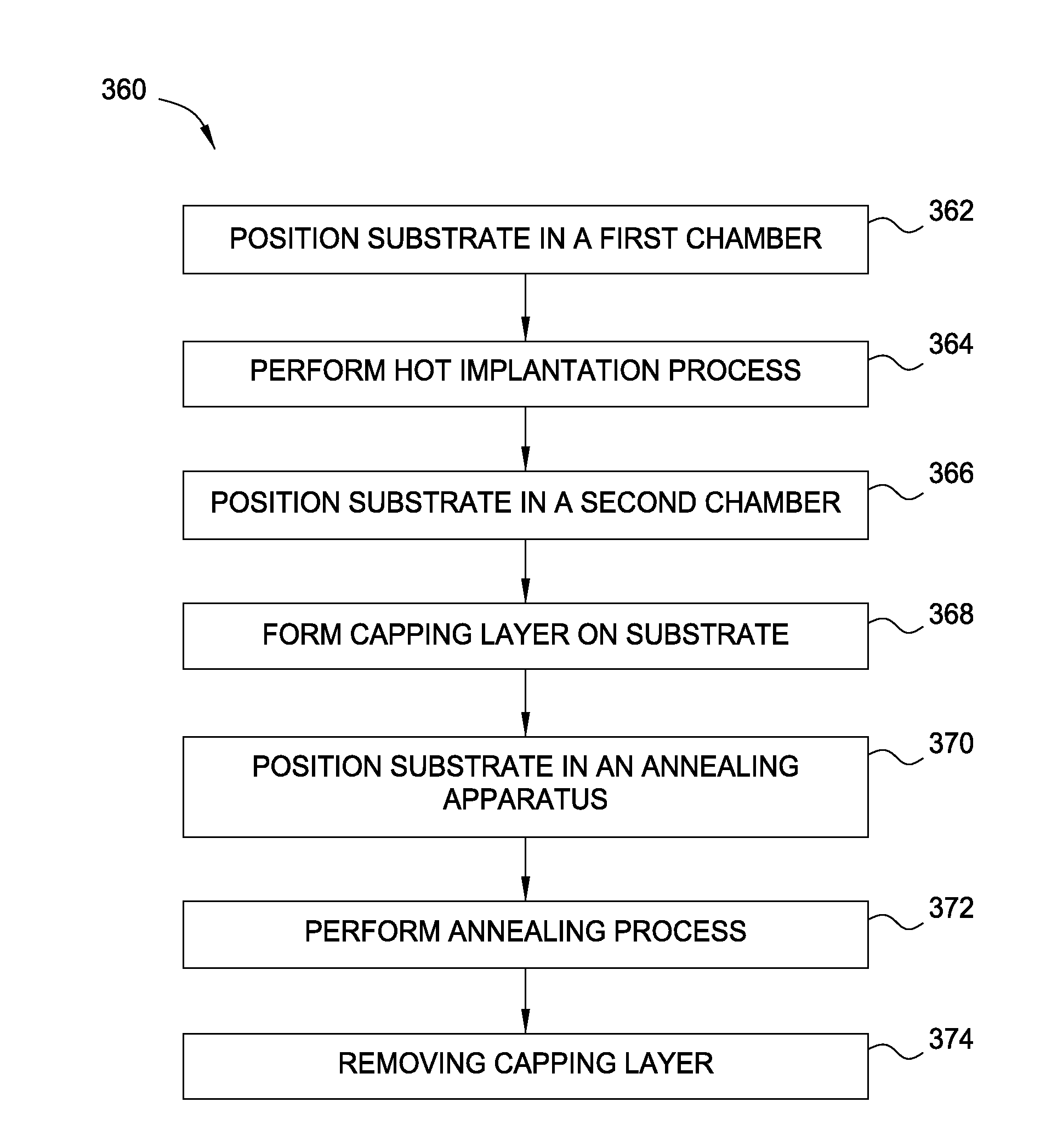
[0022]Embodiments of the present disclosure generally relate to doping and annealing substrates. The substrates may be doped during a hot implantation process, and subsequently annealed using a nanosecond annealing process. The combination of hot implantation and nanosecond annealing reduces lattice damage of the substrates and facilitates a higher dopant concentration near the surface of the substrate to facilitate increased electrical contact with the substrate. An optional capping layer may be placed over the substrate to reduce outgassing of dopants or to control dopant implant depth.

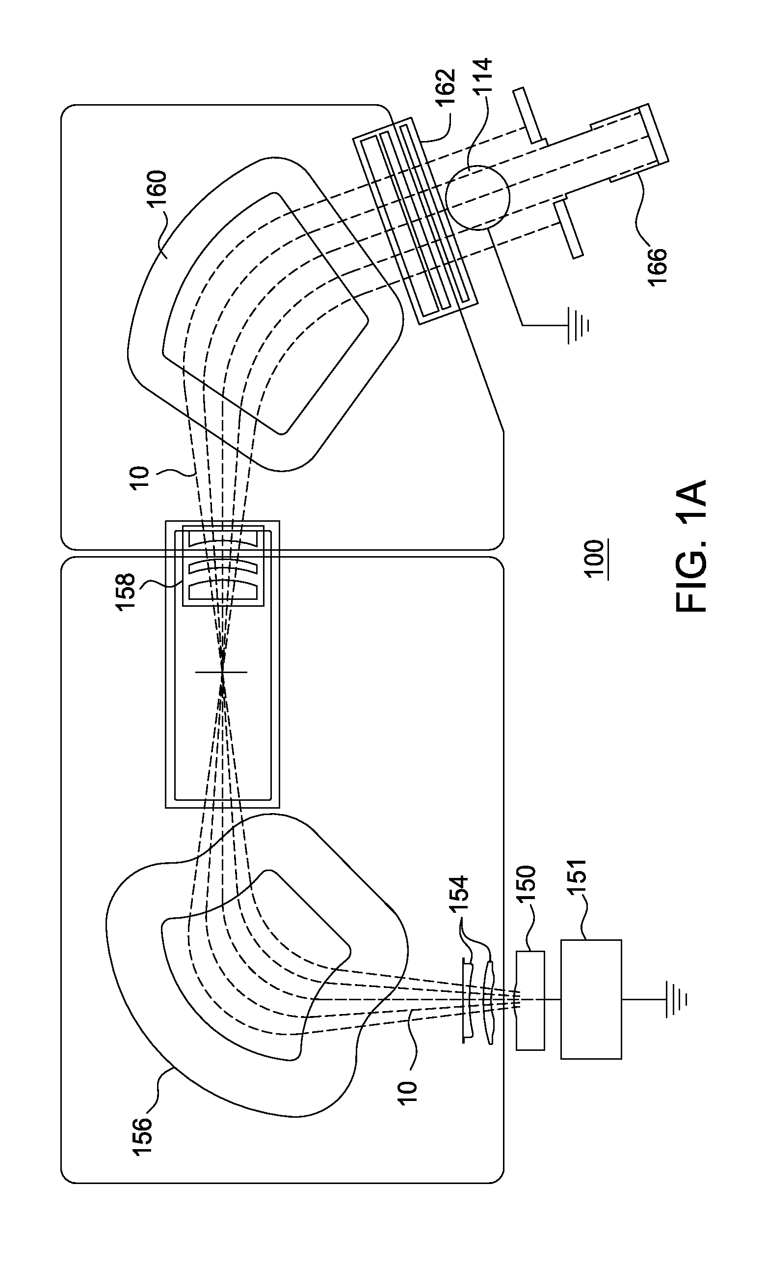
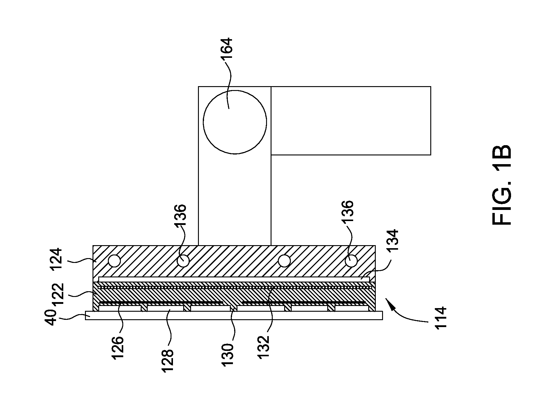
[0023]FIG. 1A depicts an on implanter system 100 in which techniques for temperature-controlled ion implantation (e.g., a hot implant) may be performed in accordance with embodiments of the present disclosure. The ion implanter system 100 may comprise an on source 150, biased to a potential by a power supply 151, and a series of beam-line components through which an ion beam 10 passes. The series of...


PUM

PropertyMeasurementUnit
temperatureaaaaaaaaaa

Abstract

Embodiments of the present disclosure generally relate to doping and annealing substrates. The substrates may be doped during a hot implantation process, and subsequently annealed using a nanosecond annealing process. The combination of hot implantation and nanosecond annealing reduces lattice damage of the substrates and facilitates a higher dopant concentration near the surface of the substrate to facilitate increased electrical contact with the substrate. An optional capping layer may be placed over the substrate to reduce outgassing of dopants or to control dopant implant depth.

Description

CROSS-REFERENCE TO RELATED APPLICATIONS[0001]This application claims benefit of U.S. Provisional Patent Application Ser. No. 61 / 887,587, filed Oct. 7, 2013, which is herein incorporated by reference.BACKGROUND OF THE DISCLOSURE[0002]1. Field of the Disclosure[0003]Embodiments of the disclosure generally relate to doping and annealing substrates, such as semiconductor substrates.[0004]2. Description of the Related Art[0005]Group III-V or II-V compounds are finding greater importance in the development and fabrication of a variety of semiconductor devices, such as light emitting diodes (LEDs), laser diodes (LDs), and logic circuit devices such as field effect transistors (FETs). In these devices, a plurality of semiconductor layers having different mixed crystal compositions are layered together to obtain intended optical and electrical characteristics.[0006]However, growing a low resistivity, high quality p-type Group III-V compound on a substrate with a desired doping profile has pr...

Claims


Application Information

Patent Timeline
Patent Type & Authority Applications(United States)
IPC IPC(8): H01L21/265H01L21/324
CPCH01L21/3245H01L21/26546
Inventor SRINIVASAN, SWAMINATHAN T.KHAJA, FAREEN ADENI
Owner APPLIED MATERIALS INC
Why Eureka
Try Eureka