Fabrication method of sic-based hemt device

A device and thin film technology, which is applied in the field of SiC-based high-mobility transistor device preparation, can solve the problems of low impurity diffusion coefficient, large crystal damage, and insufficient mobility, so as to improve mobility and reduce lattice damage.

Active Publication Date: 2018-04-27
INST OF SEMICONDUCTORS - CHINESE ACAD OF SCI
View PDF4 Cites 0 Cited by
  • Summary
  • Abstract
  • Description
  • Claims
  • Application Information

AI Technical Summary

Problems solved by technology

[0003] SiC is currently the only one that can be oxidized to form SiO 2 compound semiconductors, however in SiC and SiO 2 There is a high interface state density at the interface, which not only reduces the conductive carriers in the channel of SiC-based MOS devices, but also forms scattering centers to further reduce the channel mobility, resulting in high on-resistance and low operating frequency of the device.
Even if there are devices such as JFETs to avoid MOS interfaces, since the diffusion coefficient of impurities in SiC is very low, it is often doped by ion implantation, and the activation temperature of implanted ions is quite high, which will cause large crystal damage. Therefore the mobility is not high enough

Method used


Image

  • Fabrication method of sic-based hemt device
  • Fabrication method of sic-based hemt device
  • Fabrication method of sic-based hemt device

Examples


Embodiment Construction

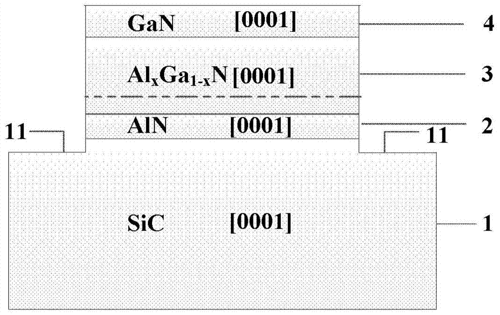
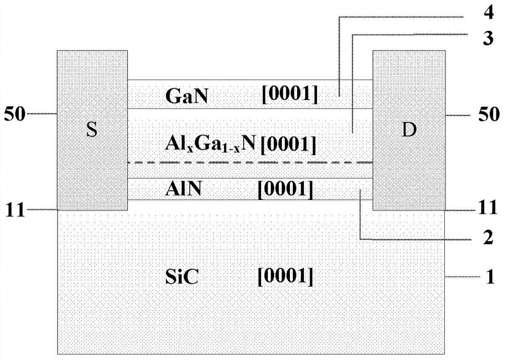
[0025] see figure 1 and refer to Figure 2-Figure 7 , the invention provides a method for preparing a HEMT device based on a SiC material, comprising the following steps:

[0026] Step 1: cleaning the SiC substrate 1, specifically:

[0027] a. Use acetone and ethanol to ultrasonically clean 3 times in sequence, and then rinse with deionized water.

[0028] b. Boiling the SiC substrate 1 after organic ultrasonication in concentrated sulfuric acid and hydrogen peroxide solution for at least 10 minutes.

[0029] c. Boil the substrate 1 that has been boiled with concentrated sulfuric acid for more than 10 minutes in sequence with No. 1 liquid and No. 2 liquid, then rinse it with deionized water and blow it dry with nitrogen for later use. The No. 1 liquid is ammonia water, hydrogen peroxide and The mixed solution of deionized water, by volume ratio ammonia water: hydrogen peroxide: deionized water=1:2:5, the No. 2 liquid is the mixed solution of hydrochloric acid, hydrogen pero...


PUM

PropertyMeasurementUnit
thicknessaaaaaaaaaa
thicknessaaaaaaaaaa
thicknessaaaaaaaaaa

Abstract

The invention discloses a SiC-based HEMT device manufacturing method, which comprises steps: a SiC substrate is cleaned; an AlN thin film is deposited on the SiC substrate; an AlxGa(1-x)N thin film is deposited on the AlN thin film; a GaN thin film is deposited on the AlxGa(1-x)N thin film; ICP dry etching is carried out at two sides of the AlN thin film, the AlxGa(1-x)N thin film and the GaN thin film to form a mesa; four layers of metal Ti / Al / Ni / Au are manufactured in the mesa, annealing is carried out, and a substrate is formed; a first Si3N4 passivation layer is deposited on the substrate; a window is photoetched, and a gate metal electrode is deposited in the window; a second Si3N4 passivation layer is then deposited on the first Si3N4 passivation layer and the gate metal electrode; and the first Si3N4 passivation layer and the second Si3N4 passivation layer on the four layers of metal Ti / Al / Ni / Au and the gate metal electrode are etched, the metal is interconnected, and device manufacturing is completed. A dielectric constant is high, spontaneous polarization is high, a critical electric field is high, and heterogeneous material is matched with lattice.

Description

technical field [0001] The invention relates to a method for obtaining two-dimensional electron gas in a SiC material, in particular to a method for preparing a SiC-based high-mobility transistor (HEMT) device. Background technique [0002] The third-generation semiconductor silicon carbide (SiC) has superior physical and electrical properties, such as wide band gap, high breakdown field strength, and high thermal conductivity. Therefore, SiC-based switching devices surpass the limit of Si power devices and occupy an absolute advantage in the fields of high-power, high-frequency, and high-temperature power electronics. [0003] SiC is currently the only one that can be oxidized to form SiO 2 compound semiconductors, however in SiC and SiO 2 There is a high interface state density at the interface, which not only reduces the conductive carriers in the channel of SiC-based MOS devices, but also forms scattering centers to further reduce the channel mobility, resulting in hig...

Claims


Application Information

Patent Timeline
Patent Type & Authority Patents(China)
IPC IPC(8): H01L21/335
CPCH01L29/66431
Inventor 申占伟张峰赵万顺王雷闫果果刘兴昉孙国胜曾一平
Owner INST OF SEMICONDUCTORS - CHINESE ACAD OF SCI
Why Eureka
Try Eureka