Enhancement-Mode GaN MOSFET with Low Leakage Current and Improved Reliability

a gan mosfet and low leakage current technology, applied in the field of gan mosfets, can solve the problems of reducing the long-term reliability of the gan device, reducing the number of trapping sites at the junction, and high leakage current passing through the algan barrier layer

Active Publication Date: 2011-08-04
NAT SEMICON CORP
View PDF9 Cites 16 Cited by
  • Summary
  • Abstract
  • Description
  • Claims
  • Application Information

AI Technical Summary

Problems solved by technology

One problem with reducing the thickness of the AlGaN barrier layer is that high levels of leakage current can pass through the AlGaN barrier layer to the gate, which is conventionally implemented as a Schottky contact.
One problem with all of these deposited oxides, including SiO2, is that these deposited oxides have a high density of interface states (e.g., greater than 4×10¹¹ / cm2) that results in a large number of trapping sites at the junction between the gate insulation layer and the AlGaN barrier layer.
Large numbers of trapping sites lead to the breakdown of the gate insulation layer which, in turn, reduces the long-term reliability of the GaN devices.

Method used


Image

  • Enhancement-Mode GaN MOSFET with Low Leakage Current and Improved Reliability
  • Enhancement-Mode GaN MOSFET with Low Leakage Current and Improved Reliability
  • Enhancement-Mode GaN MOSFET with Low Leakage Current and Improved Reliability

Examples


Embodiment Construction

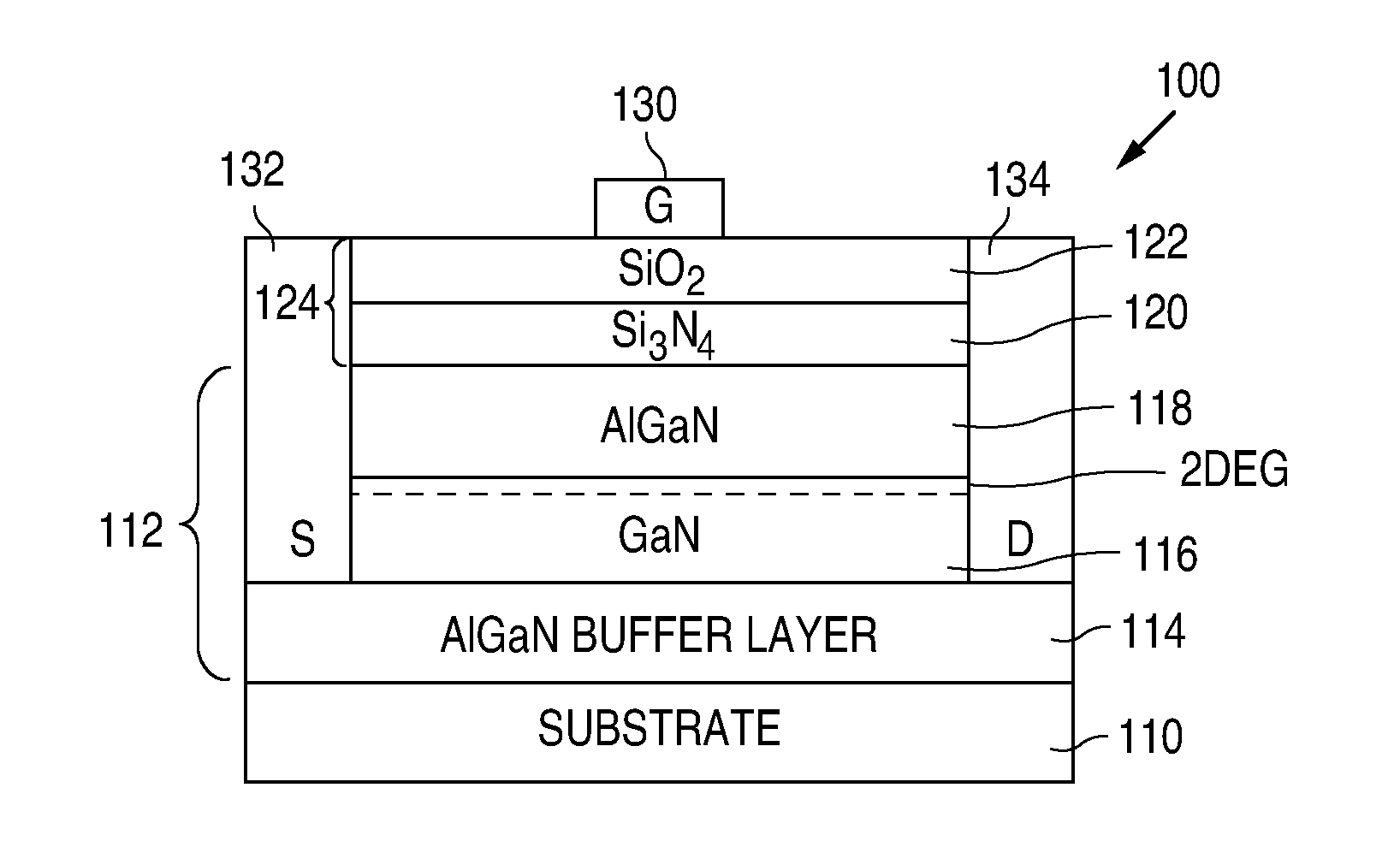
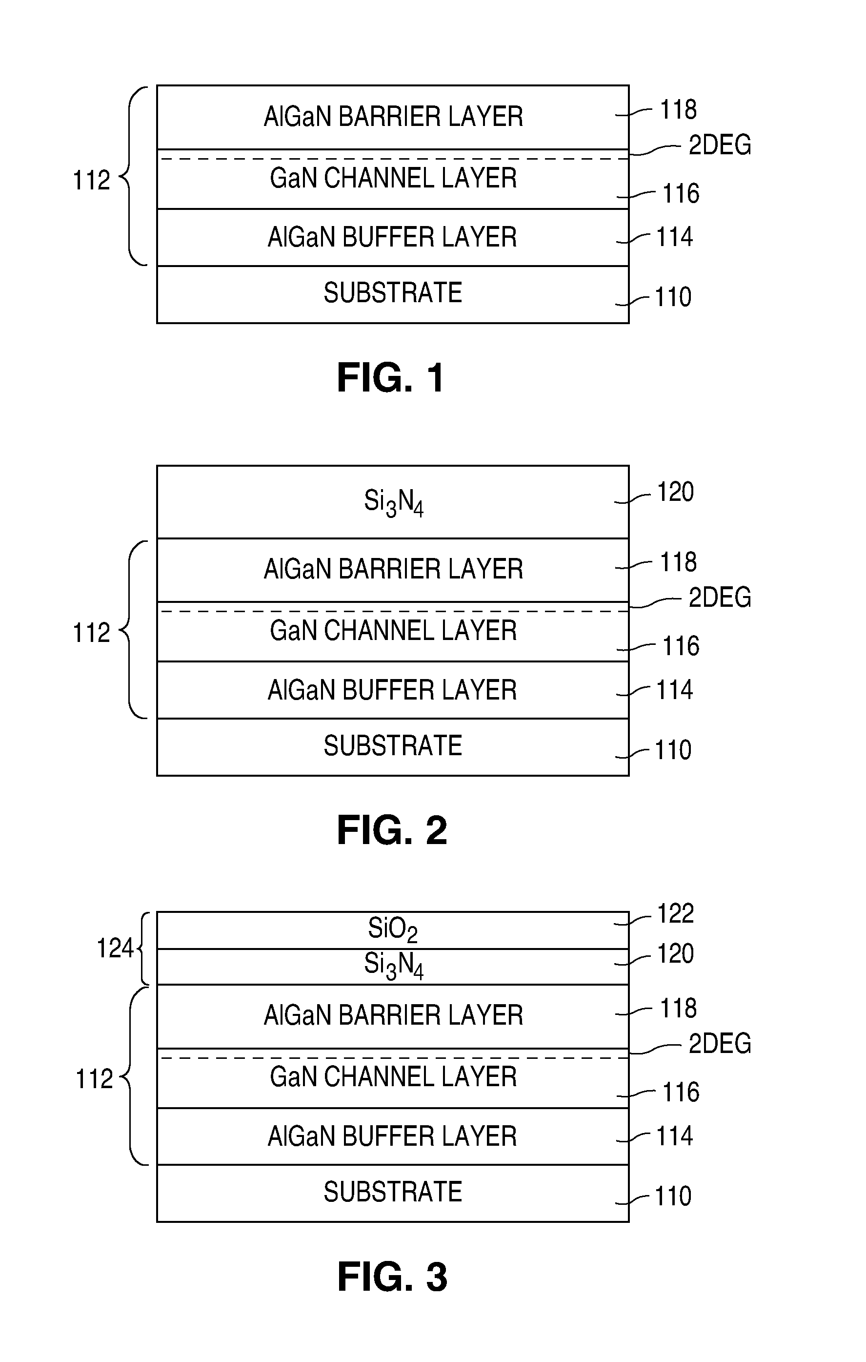
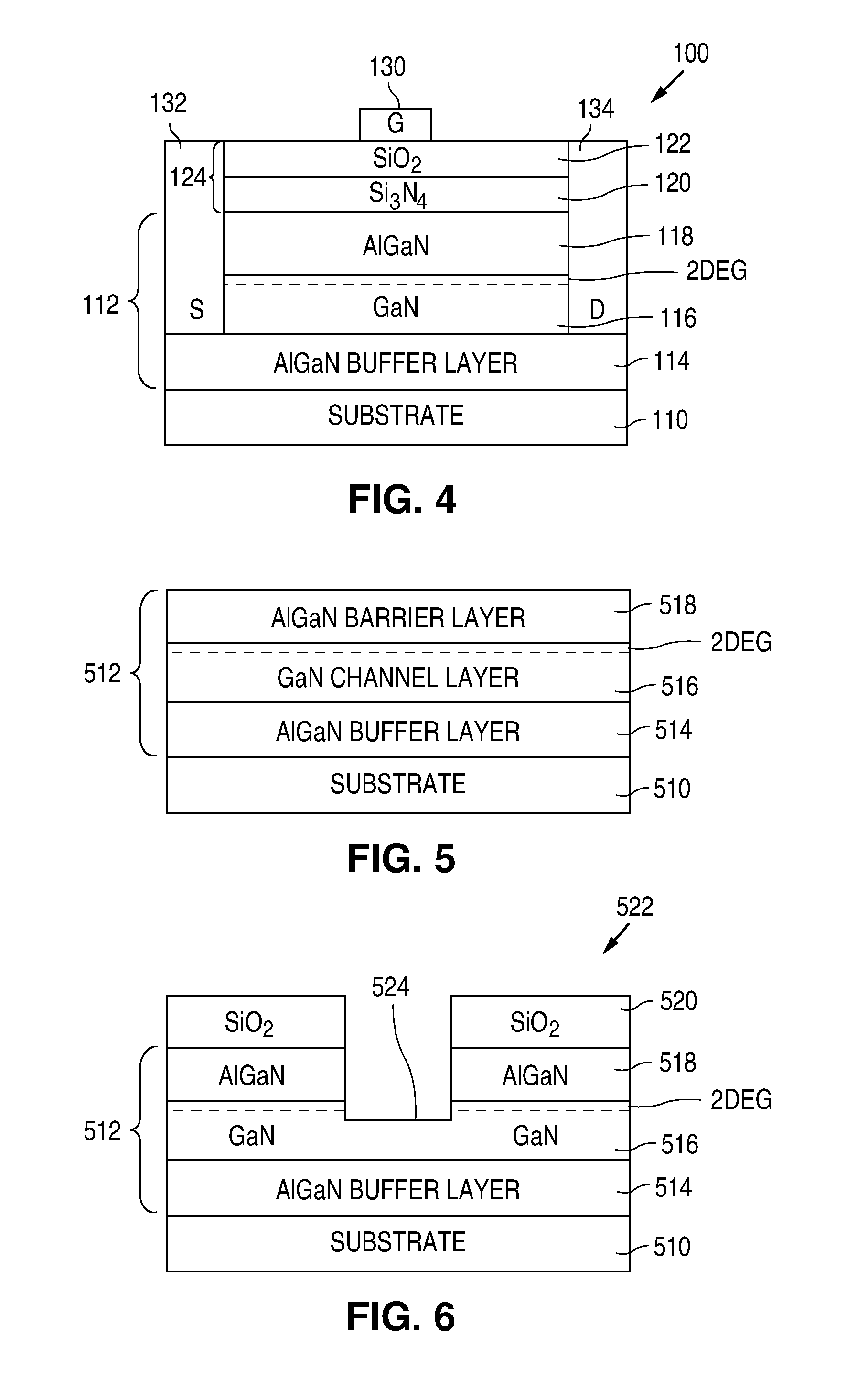
[0015]FIGS. 1-4 show a series of cross-sectional views that illustrate an example of a method of forming an enhancement-mode GaN MOSFET 100 in accordance with the present invention. As described in greater detail below, the method of the present invention forms a SiO2 / Si3N4 gate insulation layer on an AlGaN barrier layer (or optional InAlGaN barrier layer) which significantly reduces the formation of interface states at the junction between the gate insulation layer and the barrier layer. Reducing the density of interface states significantly reduces the number of trapping sites which, in turn, improves the long-term reliability on the GaN devices.

[0016]As shown in FIG. 1, the method of the present invention utilizes a conventionally-formed semiconductor substrate 110. Substrate 110 can be implemented as an insulating substrate or with a highly resistive material such as silicon (e.g., ), sapphire, or silicon carbide. As further shown in FIG. 1, the method of the present invention b...


PUM


Abstract

An enhancement-mode GaN MOSFET with a low leakage current and an improved reliability is formed by utilizing a SiO2/Si3N4 gate insulation layer on an AlGaN (or InAlGaN) barrier layer. The Si3N4 portion of the SiO2/Si3N4 gate insulation layer significantly reduces the formation of interface states at the junction between the gate insulation layer and the barrier layer, while the SiO2 portion of the SiO2/Si3N4 gate insulation layer significantly reduces the leakage current.

Description

BACKGROUND OF THE INVENTION[0001]1. Field of the Invention[0002]The present invention relates to GaN MOSFETs and, more particularly, to an enhancement-mode MOSFET with low leakage current and improved reliability.[0003]2. Description of the Related Art[0004]GaN MOSFETS are well known in the art, and are of utilized in high power, high frequency, and high temperature applications. GaN MOSFETS are typically based on the formation of a heterojunction between a GaN region, typically known as the channel layer, and an overlying AlGaN region, typically known as a barrier layer. The GaN channel layer and the AlGaN barrier layer have different band gaps that induce the formation of a two-dimensional electron gas (2DEG) that lies at the junction between the[0005]GaN channel layer and the AlGaN barrier layer and extends down into the GaN channel layer.[0006]The 2DEG, which functions as the “channel” of the transistor, produces a high concentration of electrons which causes a conventionally-fo...

Claims


Application Information

Patent Timeline
Patent Type & Authority Applications(United States)
IPC IPC(8): H01L29/778H01L21/335
CPCH01L21/28264H01L29/1054H01L29/2003H01L29/205H01L29/513H01L29/66431H01L29/66462H01L29/66522H01L29/7787H01L21/02458H01L21/0254H01L29/518
Inventor RAMDANI, JAMAL
Owner NAT SEMICON CORP
Why Eureka
Try Eureka